Change even page title here
Chapter 5 Configuration of the
5.1Modifications for use with MB90470 / MB90480 series
Some modifications have to be done in order to use the
1.Check that U6 is MAX3232CPE
2.Change R6 470 => 390 Ohm. Check that output voltage of U3 is 3.3V (JP2)
3.Disassemble C10 (100nF)
4.Connect J4- Pin 27 to JP10- Pin 2 (SIN)
5.Connect J4- Pin 28 to JP9- Pin 2 (SOT)
6.Connect J5- Pin 80 to GND (X0A) if no
Otherwise
7.Remove JP1. Connect JP1- Pin 2 to JP2- Pin 1
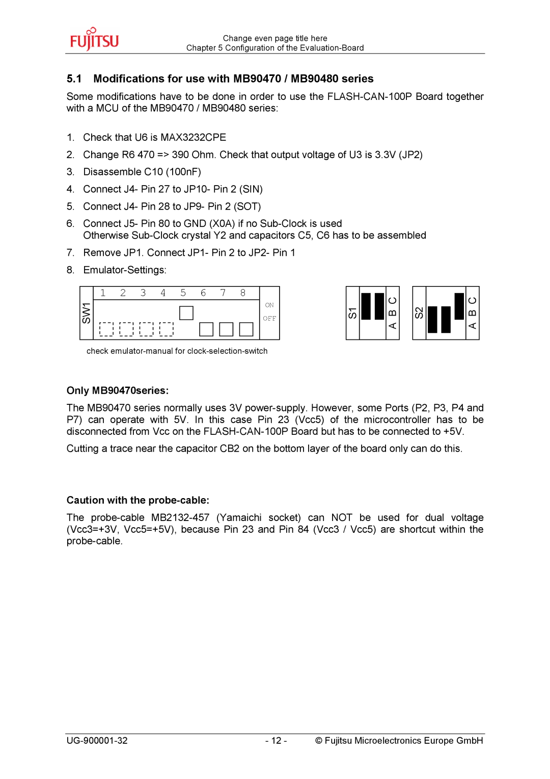
8.
SW1 | 1 | 2 | 3 | 4 |
| 5 | 6 | 7 |
| 8 |
| ON | ||||||
|
|
|
|
|
|
|
|
|
|
|
|
|
|
|
|
| ||
|
|
|
|
|
|
|
|
|
|
|
|
|
|
|
| |||
|
|
|
|
|
|
|
|
|
|
|
|
|
|
|
|
| OFF | |
|
|
|
|
|
|
|
|
|
|
|
|
|
|
| ||||
|
|
|
|
|
|
|
|
|
|
|
|
|
|
| ||||
|
|
|
|
|
|
|
|
|
|
|
|
|
|
|
|
|
|
|
|
|
|
|
|
|
|
|
|
|
|
|
|
|
|
|
|
|
|
check
S1![]()
![]()
A B C
S2![]()
![]()
![]()
A B C
Only MB90470series:
The MB90470 series normally uses 3V
Cutting a trace near the capacitor CB2 on the bottom layer of the board only can do this.
Caution with the
The
- 12 - | © Fujitsu Microelectronics Europe GmbH |
