Appendix

A. Connector pin

assignments


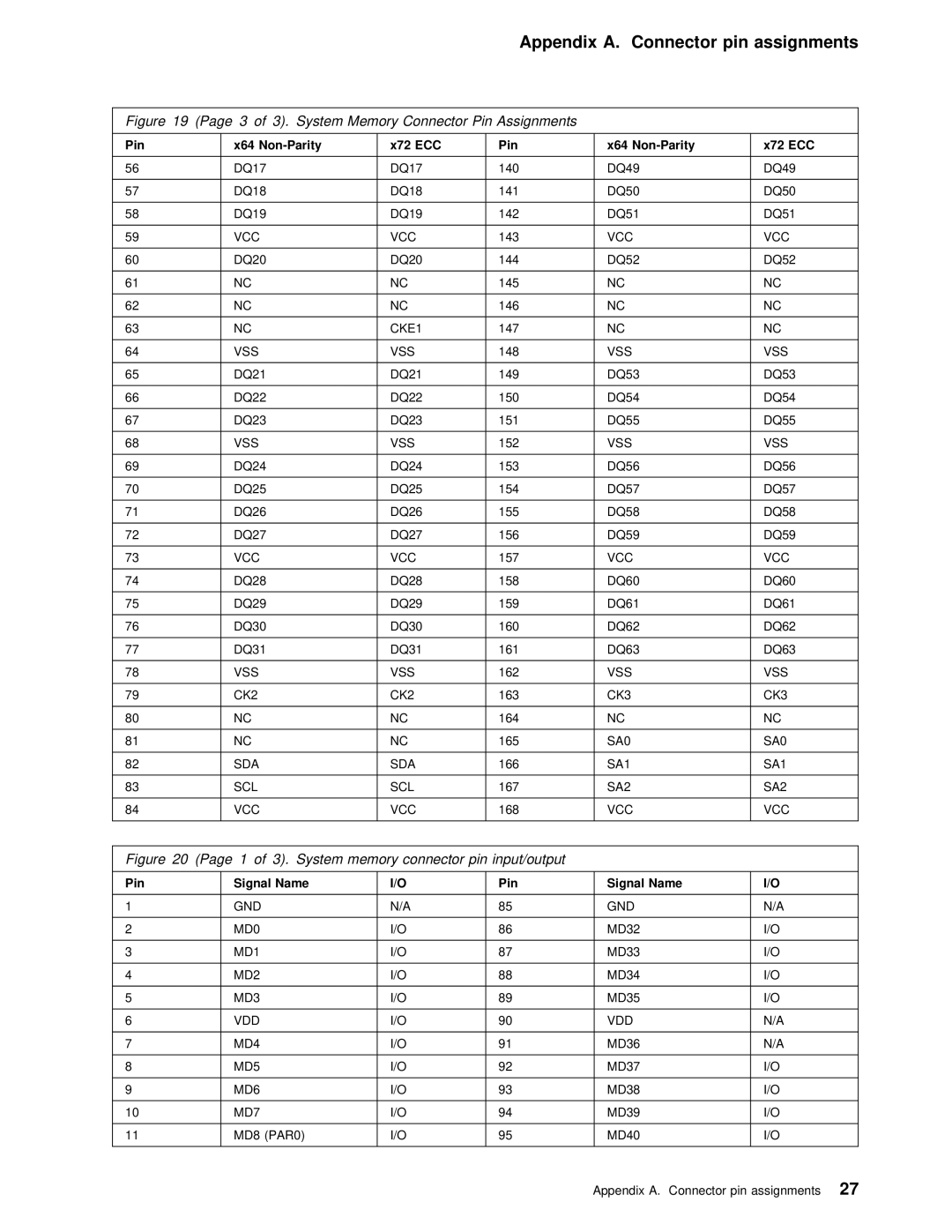
Figure

19


(Page

3

of

3).

System Memory Connector Pin Assignments


Pin


x64

Non-Parity


x72 ECC

Pin


x64

Non-Parity


x72 ECC


56


DQ17


DQ17

140


DQ49


DQ49


57


DQ18


DQ18

141


DQ50


DQ50


58


DQ19


DQ19

142


DQ51


DQ51


59


VCC


VCC

143


VCC


VCC


60


DQ20


DQ20

144


DQ52


DQ52


61


NC


NC

145


NC


NC


62


NC


NC

146


NC


NC


63


NC


CKE1

147


NC


NC


64


VSS


VSS

148


VSS


VSS


65


DQ21


DQ21

149


DQ53


DQ53


66


DQ22


DQ22

150


DQ54


DQ54


67


DQ23


DQ23

151


DQ55


DQ55


68


VSS


VSS

152


VSS


VSS


69


DQ24


DQ24

153


DQ56


DQ56


70


DQ25


DQ25

154


DQ57


DQ57


71


DQ26


DQ26

155


DQ58


DQ58


72


DQ27


DQ27

156


DQ59


DQ59


73


VCC


VCC

157


VCC


VCC


74


DQ28


DQ28

158


DQ60


DQ60


75


DQ29


DQ29

159


DQ61


DQ61


76


DQ30


DQ30

160


DQ62


DQ62


77


DQ31


DQ31

161


DQ63


DQ63


78


VSS


VSS

162


VSS


VSS


79


CK2


CK2

163


CK3


CK3


80


NC


NC

164


NC


NC


81


NC


NC

165


SA0


SA0


82


SDA


SDA

166


SA1


SA1


83


SCL


SCL

167


SA2


SA2


84


VCC


VCC

168


VCC


VCC


Figure

20

(Page

1

of

3).

System memory connector pin input/output


Pin


Signal


Name


I/O

Pin


Signal

Name


I/O


1


GND


N/A

85


GND


N/A


2


MD0


I/O

86


MD32


I/O


3


MD1


I/O

87


MD33


I/O


4


MD2


I/O

88


MD34


I/O


5


MD3


I/O

89


MD35


I/O


6


VDD


I/O

90


VDD


N/A


7


MD4


I/O

91


MD36


N/A


8


MD5


I/O

92


MD37


I/O


9


MD6


I/O

93


MD38


I/O


10


MD7


I/O

94


MD39


I/O


11


MD8

(PAR0)


I/O

95


MD40


I/O


Appendix A. Connector pin assignments27

Page 35
Image 35
IBM 6278, 6288, 6268 manual Assignments, Connector pin, System memory connector pin input/output

6278, 6268, 6288 specifications

The IBM 6278, 6288, and 6268 are part of IBM's extensive lineup of mid-range computers, specifically tailored for business environments in the late 1980s and early 1990s. These systems were designed to handle substantial data processing tasks, facilitating efficient business operations with robust performance and reliability.

The IBM 6278 was notable for its high-performance capabilities, making it suitable for a variety of applications ranging from transaction processing to complex computations. One of the main features of the 6278 was its multiprocessing capability, which allowed it to run multiple tasks concurrently. This was achieved through a combination of advanced hardware and software that optimized performance and resource allocation.

Similarly, the IBM 6288 was recognized for its versatility and scalability. This system incorporated enhanced memory management and was capable of handling larger workloads than its predecessors. The 6288 was designed with user-friendly interfaces and supported various input/output devices, making it easier for organizations to integrate into existing IT infrastructures. Additionally, it provided improved connectivity options, essential for modern networking needs at the time.

The IBM 6268, on the other hand, offered a balance between cost and performance, appealing to smaller businesses or those with less intensive data processing requirements. Despite being less powerful than the 6278 and 6288, the 6268 still managed to include essential features such as reliable data storage, effective processing speed, and compatibility with IBM's extensive software ecosystem.

All three models utilized IBM's proprietary operating systems, which were well-known for their robustness and security features. They were built with technologies such as error detection and correction, ensuring the integrity of data processing tasks. The architecture of these systems also allowed for easy upgrades, enabling businesses to expand their capabilities without a complete overhaul of their IT infrastructure.

In summary, the IBM 6278, 6288, and 6268 represented a significant advancement in mid-range computing technology during their era. Their main features encompassed multiprocessing, scalability, and user-friendly interfaces, making them valuable assets for businesses seeking reliable and efficient computing solutions. These systems laid the groundwork for future innovations in business computing, and despite their age, they remain a significant part of IBM's legacy in the computing industry.