EM78P468N/L
Elan Microelectronics Corporation
Contents
Infrared Remote Control Application/PWM Waveform Generate
Doc. Version Revision Description Date
Appendix
Contents Product Specification V1.5
Bit Microcontroller
Features
General Description
Pin QFP Pin Lqfp
Pin Assignment
System Block Diagram
Block Diagram
Pin Description for Package of QFP64 and LQFP64
Symbol Pin No Type Function
Pin Description
SEG11~SEG14
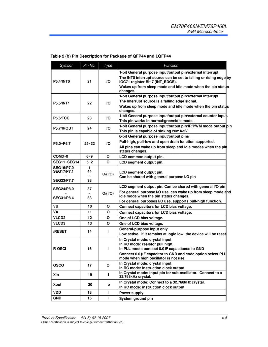
Pin Description for Package of QFP44 and LQFP44
1 R0/IAR Indirect Addressing Register
2 R1/TCC Timer Clock Counter
Function Description
Operational Registers
On-ChipProgrammemory
Bit 0 C Carry flag
4 R3/SR Status Register
Bits 6 ~ 5 PS1 ~ 0 Page select bits
Bit 2 Z Zero flag
8 R7/Port 7 Port 7 I/O Data Register
5 R4/RSR RAM Select Register
6 R5/Port 5 Port 5 I/O Data and Page of Register Select
7 R6/Port 6 Port 6 I/O Data Register
Lcdtype = 0 a type waveform Lcdtype = 1 B type waveform
Bit 4 Lcden LCD enable bit
9 R8/Port 8 Port 8 I/O Data Register
10 R9/LCDCR LCD Control Register
RB/LCDDB LCD Data Buffer
RC/CNTER Counter Enable Register
11 RA/LCDADDR LCD Address
Example Fs=32.768K
14 RD/SBPCR System, Booster and PLL Control Register
Address 0Dh
Main clock
Address 0Eh
15 RE/IRCR IR and Port 5 Setting Control Register
Bit Microcontroller CPU Operation Mode
Address 0Fh
16 RF/ISR Interrupt Status Register
Address 10h~3Fh R10~R3F General Purpose Register
Address 05h, Bit 0 of R5 =
Special Purpose Registers
Accumulator
6 IOC90/RAMADDR 128 Bytes RAM Address
3 IOC60/P6CR Port 6 I/O Control Register
4 IOC70/P7CR Port 7 I/O Control Register
5 IOC80/P8CR Port 8 I/O Control Register
IOCD0/HPWTPR High-Pulse Width Timer Preset Register
IOCB0/CNT1PR Counter 1 Preset Register
IOCC0/CNT2PR Counter 2 Preset Register
Bits 6, 5, 4 Not used
IOCE0/LPWTPR Low-Pulse Width Timer Preset Register
IOCF0/IMR Interrupt Mask Register
TCC Rate
14 IOC71/TCCCR TCC Control Register
Bit 7 Intedge
Bits 3~0 PSRE, TCCP2 ~ TCCP0 TCC prescaler bits
WDT Rate
15 IOC81/WDTCR WDT Control Register
16 IOC91/CNT12CR Counters 1, 2 Control Register
Bits 7 ~ 4 Not used
Counter 1 Scale
IOCA1/HLPWTCR High/Low Pulse Width Timer Control Register
Low-pulse Width Timer Scale
High-pulse Width Timer Scale
IOCE1/P6PL Port 6 Pull Low Control Register
IOCB1/P6PH Port 6 Pull-high Control Register
IOCC1/P6OD Port 6 Open Drain Control Register
IOCD1/P8PH Port 8 Pull High Control Register
MUX
TCC and WDT Prescaler
TCC Setting Flowchart
Bit Microcontroller WDT Setting Flowchart
I/O Ports
Reset and Wake-up
Bit Microcontroller Summary of Registers Initialized Values
Address Name Reset Type Bit
INT Psre TCCP2 TCCP1 TCCP0
Name Reset Type Bit
Wake-up Signal Sleep Mode Idle Mode Green Mode Normal Mode
Oscillator Modes
Phase Lock Loop PLL Mode
Oscillator
Oscillator Source Oscillator Type Frequency C1 pF C2 pF
Crystal Oscillator/Ceramic Resonators Crystal
Main clock Example Fs=32.768KHz
Pin Rext Average Fosc 5V, 25 C Average Fosc 3V, 25 C
Power-on Considerations
RC Oscillator Mode with Internal Capacitor
RC Oscillator Frequencies
Residue-Voltage Protection
External Power-on Reset Circuit
13 Interrupt Back-up
Interrupt
Bits 6 ~ 5 DS1 ~ DS0 LCD duty select
LCD Driver
1 R9/LCDCR LCD Control Register
Bits 4 ~ 0 LCDA4 ~ LCDA0 LCD RAM address
2 RA/LCDADDR LCD Address
3 RB/LCDDB LCD Data Buffer
Bits 7 ~ 5 Not used, fixed to
Bit 2 ~ 1 BF1 ~ 0 LCD booster frequency select bits
4 RD/SBPCR System, Booster and PLL Control Registers
External circuit for 1/2 Bias
Boosting circuits connection for LCD voltage
External circuit for 1/3 Bias
16 LCD Waveform for 1/2 Bias, 1/2 Duty
18 LCD Waveform for 1/3 Bias, 1/3 Duty
⋅ 1 + decimal C ounter Preset Value Iocc 0 ⋅ prescaler
Infrared Remote Control Application/PWM Waveform Generate
21 LGP=0, Irout Pin Output Waveform
23 LGP=0, Irout Pin Output Waveform
IR application
Bit Microcontroller IR/PWM Function Enable Flowchart
Bits12~10 Word
Code Options
Bits 12 ~ 10 Not used
Word
PR1PR0Protect
Instruction Set
Bits 2~0 PR2~PR0 Protect Bit
Convention
Binary Instruction Hex Mnemonic Operation Status
JZA
Binary Instruction Hex Mnemonic Operation Status Affected
AC Test Input/Output Waveform
Timing Diagram
Absolute Maximum Ratings
Items Symbol Condition Rating Min Max Unit
Ta= -40 C ~85 C, VDD= 5.0V, GND=
Electrical Characteristic
DC Electrical Characteristics
Symbol Parameter Condition Min Typ Max Unit
Ta= -40C ~85 C, VDD= 3.0V, GND=
Ta=- 40C ~ 85 C, VDD=5V±5%, GND=0V
AC Electrical Characteristics
Symbol Parameter Conditions Min Typ Max Unit
Vih/Vil /RESET pins with schmitt inverter
Device Characteristic
Vih/Vil Port 7, Port 8 All Input pins with schmitt inverter
P5.7 Voh/Ioh VDD=5V, IROCS=1 P5.7 Voh/Ioh VDD=3V, IROCS=1
80 P5.7 Voh/Ioh VDD=5V, IROCS=0 Max Typ +25
Setup time from Power on Reset
= 51 K
13 Typical Eric OSC Frequency vs. Temperature Xin Pin
VDD=5V
Typical ICC2 vs. Temerature
Typical ICC1 vs. Temerature
Typical ISB vs. Temerature
22 Operating Voltage under Temperature Range of 0C to 70C
Application Circuit
EM78P468NxS/xJ
Package Type
Name Package Type Pin Count Package Size
QFP
Package Information
900 100 BSC 00 REF
Lqfp
Min Normal Max 30TYP 15TYP
Program Pin Name IC Pin Name QFP-64 QFP-44
Wiring diagram is for Elan Dwtr
EM78P468N/L Program Pin List
Main oscillator RC mode, Sub oscillator Crystal
Main oscillator Crystal mode, Sub oscillator Crystal mode
Main oscillator PLL mode, Sub oscillator Crystal mode
ICE 468XA Oscillator Circuit JP
Bit Microcontroller
VLCD3 GND Osco
ICE 468XA Output Pin Assignment JP
Test Category Test Conditions
Quality Assurance and Reliability
Address Trap Detect
Contents III

