SG-80 Series
Page
Table of Contents
Appendix A. How to Get Technical Support
Chapter Driver Installation
Features & Specifications
Product List
Model Chipset Features
Back Panel I/O
Miscellaneous
Layout Diagram SG-80
Layout Diagram SG-81
Connectors Description
Jumpers & Connectors Description
Jumpers Description Default Setting
SG-80 Series
CPU Socket
Hardware Setup
Total System Memory
System Memory
Dimm Module Total Memory
ATX Power Connectors ATXPOWER, ATX12V
Connectors, Headers, and Switches
FAN Connectors CPUFAN, SYSFAN, Pwrfan
Cmos Memory Clearing Header Ccmos
Pin 2-3 shorted default Normal operation
Pin Definition
Front Panel Switches & Indicators Connection Headers PANEL1
Additional USB Port Connection Header USB3, USB4
Pin Signal Name Function
Front Panel Audio Connection Header FPIO-AUDIO1
Accelerated Graphics Port Slot AGP1
Internal Audio Source Connectors CD1, AUX1
Floppy Disk Drive Connector FDC
IDE Disk Drive Connectors IDE1, IDE2
Serial ATA connectors SATA1, SATA2
External I/O Panel
Standard Configuration
About the Setup Utility
Exits the current menu
Updating the Bios
Date and Time
Using Bios
Standard Cmos Features
IDE Channel 1/2 Master/Slave/ IDE DriveAuto
IDE Devices None
IDE HDD Auto-Detection
Video EGA/VGA
Access Mode Auto
Floppy 3 Mode Support Disabled
Drive A/Drive B 1.44M, 3.5 in./None
CPU Feature
Advanced Bios Features
Hard Disk Boot Priority
First/Second/Third Boot Device Floppy/Hard Disk/CDROM
CPU L3 Cache Enabled
Hyper-Threading Technology Enabled
Quick Power On Self Test Enabled
Small LogoEPA Show
Advanced Chipset Features
ATA 66/100 IDE Cable Msg. Enabled
Security Option Setup
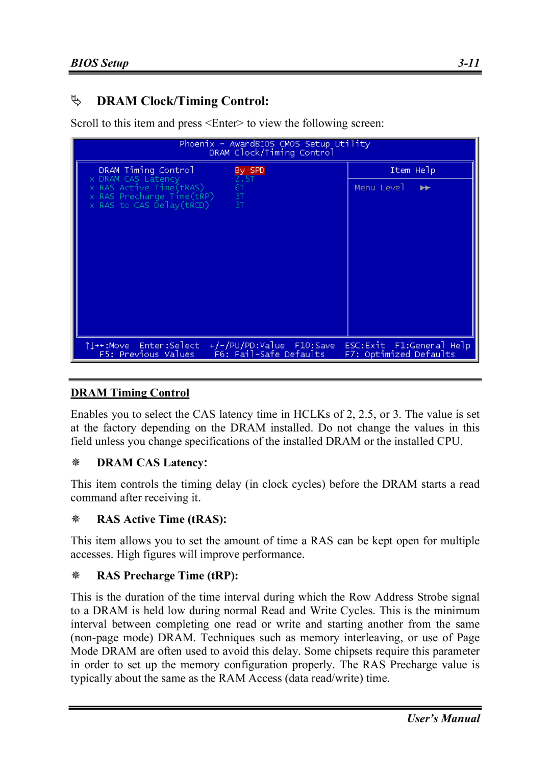
RAS Active Time tRAS
Dram Clock/Timing Control
Dram Timing Control
Dram CAS Latency
AGP & P2P Bridge Control
RAS to CAS Delay tRCD
Graphic Window WR Combin Enabled
AGP Fast Write Support Disabled
AGP Data Rate Auto
System Bios Cacheable Disabled
Video RAM Cacheable Disabled
OnChip AGP Control
OnChip IDE Device
Integrated Peripherals
Serial ATA Mode IDE
IDE DMA Transfer Access Enabled
IDE Burst Mode Enabled
OnChip Sata Controller Enabled
LAN Boot ROM Disabled
OnChip USB Controller Enabled
OnChip AC97 Controller Enabled
OnChip LAN Controller Enabled
Onboard Serial Port 1 3F8/IRQ4
Onboard FDC Controller Enabled
Parallel Port Mode ECP
Onboard SuperIO Device
Init Display First PCI Slot
Power Management Setup
ECP Mode Use DMA
Onboard 1394 Device Enabled
Wakeup By Ring Disabled
Resume by USB from S3 Disabled
Power On by PS2 Keyboard Hot Key
Power On by PS2 Mouse Disabled
Resources Controlled By AutoESCD
PnP/PCI Configurations
IRQ Resources
PCI/VGA Palette Snoop Disabled
PIRQ0 Use IRQ No. ~ PIRQ7 Use IRQ No. Auto
CPU Shutdown Temperature Disabled
System Component Characteristics
PC Health Status
Frequency Control
Load Fail-Safe Defaults Option
Auto Detect DIMM/PCI Clk Enabled
Spread Spectrum Enabled
Set Password
Load Optimized Defaults Option
Exit Without Saving
Save & Exit Setup Option
SG-80 Series
Driver Installation
Browse CD
Setup Items
Drivers
Manual Utility
User’s Manual
How to Get Technical Support
SG-80 Series
Appendix a
Jan van Riebeeckweg 15, 5928LG, Venlo
Technical Support Form