!Award BIOS Setup Utility 


 3.1.3 Chipset Features Setup
ROM PCI/ISA BIOS
CHIPSET FEATURES SETUP
AWARD SOFTWARE, INC.
|
|
|
|
|
|
|
|
|
|
|
| SDRAM | : | 3 |
|
|
|
|
|
|
|
| SDRAM RAS Precharge Time | : | 3 |
|
|
|
|
|
|
|
| SDRAM CAS Latency Time | : | 3 |
|
|
|
|
|
|
|
| SDRAM Precharge Control | : | Disabled |
|
|
|
|
|
|
|
| DRAM Data Integrity Mode | : |
|
|
|
|
|
|
| |
| System BIOS Cacheable | : | Disabled |
|
|
|
|
|
|
|
| Video BIOS Cacheable | : | Disabled |
|
|
|
|
|
|
|
| Video RAM Cacheable | : | Disabled |
|
|
|
|
|
|
|
| 8 Bit I/O Recovery Time | : | 1 |
|
|
|
|
|
|
|
| 16 Bit I/O Recovery Time | : | 1 |
|
|
|
|
|
|
|
| Memory Hole At | : | Disabled |
|
|
|
|
|
|
|
| PCI 2.1 Compliance | : | Disabled |
|
|
|
|
|
|
|
| AGP Aperture Size (MB) | : | 64 |
|
|
|
|
|
|
|
| CPU/PCI Clock (MHz) | : Default |
|
|
|
|
|
|
| |
| Spread Spectrum | : Disabled |
|
|
|
|
|
|
| |
|
|
|
|
|
|
|
|
|
|
|
|
|
|
| ESC | : | Quit | ↑ ↓ → ← | : | Select Item |
|
|
|
|
| F1 | : | Help | PU/PD/+/- | : | Modify |
|
|
|
|
| F5 | : | Old Values (Shift) F2 | : | Color |
| |
|
|
|
| F6 : Load |
|
|
| |||
|
|
|
| F7 : Load Optimal Settings |
|
|
| |||
|
|
|
|
|
|
|
|
|
|
|
|
|
|
|
|
|
|
|
|
|
|
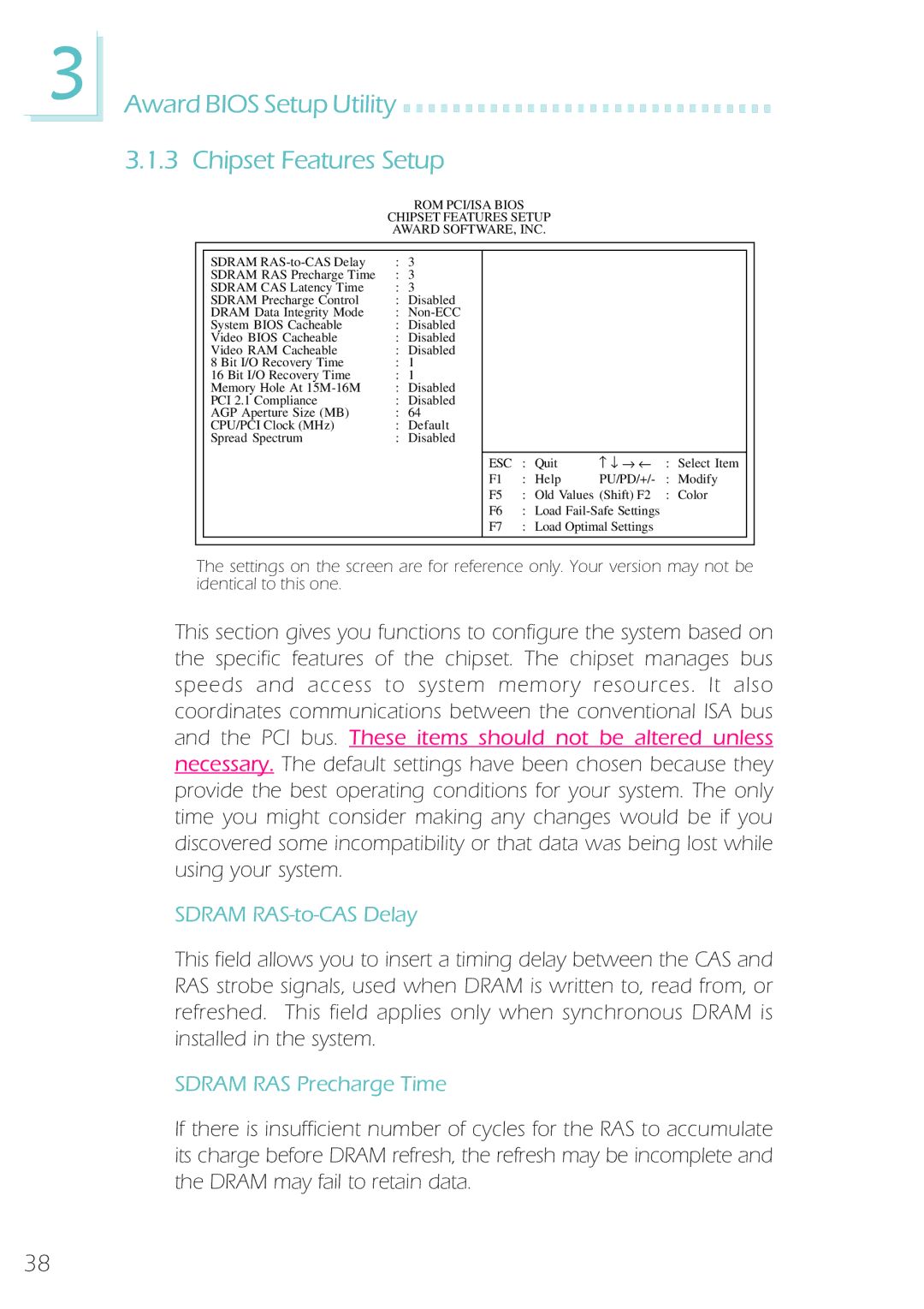
The settings on the screen are for reference only. Your version may not be identical to this one.
This section gives you functions to configure the system based on the specific features of the chipset. The chipset manages bus speeds and access to system memory resources. It also coordinates communications between the conventional ISA bus and the PCI bus. These items should not be altered unless necessary. The default settings have been chosen because they provide the best operating conditions for your system. The only time you might consider making any changes would be if you discovered some incompatibility or that data was being lost while using your system.
SDRAM RAS-to-CAS Delay
This field allows you to insert a timing delay between the CAS and RAS strobe signals, used when DRAM is written to, read from, or refreshed. This field applies only when synchronous DRAM is installed in the system.
SDRAM RAS Precharge Time
If there is insufficient number of cycles for the RAS to accumulate its charge before DRAM refresh, the refresh may be incomplete and the DRAM may fail to retain data.
38
