MVME712A, MVME712AM
MVME712A/D3
Restricted Rights Legend
Preface
Related Documentation
Document Title Motorola Publication Number
Manual Terminology
Page
Safety Summary Safety Depends On You
This equipment generates, uses, and can radiate radio
Page
Contents
Page
List of Figures
Features of the MVME712 Family Modules
Introduction
Collective Reference
Specifications
Features of the LCP2 Adapter Board
Characteristics SpeciÞcations
MVME712 Family Specifications
Cooling Requirements
FCC Compliance
General Description
Unpacking Instructions
MVME712x Module Preparation
MVME712-12 Header Locations
MVME712x Module Preparation
InstallationHardware Preparation
LocationsMVME712AFigure 2-3.Header
LMVME712AMocationsFigure 2-4.Header
DSR Line Pull Up Select Headers J8, J9, J13, J14
DCE DTE
Serial Port Configuration
Serial Port 2/Modem Port 2 Select J16, J17
Ote
Modem Port Configuration
MVME712B Module Preparation
Scsi Termination
MVME712B Connector Locations
LCP2 Adapter Connector Locations
LCP2 Adapter Board Preparation
Installation Instructions
Installing for Use with Internal Scsi Devices
Internal Scsi and Serial Port Connections
Installing the MVME712-13 and MVME712AM as a Modem
Internal Scsi and Modem Connections
MVME712B Installation
MVME712B External Scsi Connections
Hardware Preparation and Installation
MVME712 Jumpers
Interconnect Signals
LCP2 and MVME712 Connectors
From
Connectors J1, J3-J5 Interconnect Signals MVME712x
Connector P2 Interconnect Signals LCP2 Adapter
Connectors J1, J3-J5 Interconnect Signals MVME712x
Pin Signal Signal Name and Description Number Mnemonic
RTS
CTS
Connector J2 Interconnect Signals LCP2 Adapter
Connector J2 Interconnect Signals LCP2 Adapter
Prpe
GND Ground Prfault
Prack
Prbsy
GND Ground RXD1
DTR3
TXD1
GND Ground RTS1
DTR4
RTS4
GND Ground TRXC4
CTS4
DCD2
CTS2
RTS2
DTR2
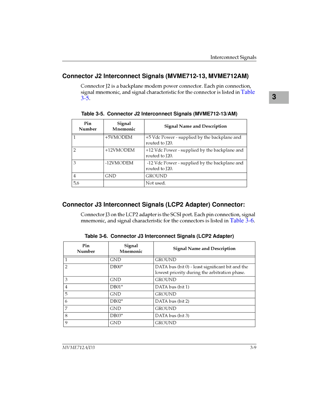
Connector J2 Interconnect Signals MVME712-13/AM
Connector J2 Interconnect Signals MVME712-13, MVME712AM
Connector J3 Interconnect Signals LCP2 Adapter Connector
Connector J3 Interconnect Signals LCP2 Adapter
GND Ground ATN
Termpwr Terminator Power
GND Ground DBP
GND Ground BSY
Connector Scsi Interface Interconnect Signals MVME712B
Scsi Interface Interconnect Signals MVME712B
GND Ground REQ
GND Ground Termpwr Terminator Power
Connector Ethernet Interconnect Signals MVME712B
Ethernet Interconnect Signals MVME712B
MAU
Connector J6 Interconnect Signals MVME712-13/AM
Connector J6 Interconnect Signals MVME712-13, MVME712AM
Connector J7 Interconnect Signals MVME712-13, MVME712AM
10. Connector J7 Interconnect Signals MVME712-13/AM
MDMRXD2
Connector J10 Interconnect Signals MVME712x
11. Connector J10 Interconnect Signals MVME712x
MDMDCD2
Connector P2 and J11 Interconnect Signals MVME712x
12. Connector P2, J11 Interconnect Signals MVME712x
Pin Number Signal Signal Name and Description J11 Mnemonic
Data bit 6 Printer
A16
A23
Connector J12 Interconnect Signals MVME712-13, MVME712AM
13. Connector J12 Interconnect Signals MVME712-13/12AM
Connector J15 Interconnect Signals MVME712x
14. Connector J15 Interconnect Signals MVME712x
Model Parts List Parts Location Drawing
Parts Lists and Locations
15. MVME712 x Module Parts List
Reference Motorola Description Designation Part Number
15. MVME712x Module Parts List
Modem kit MVME712-13 and MVME712AM
Side
MVME7121.-3FigureocationL-12 Parts
MVME712-13 Parts Location Drawing Primary Side
DrawingFigure 3-3. MVME712A Parts LocationPrimary Side
1532
PartsMVME712AMFigure 3-4.Location Drawing Primary Side
CR3 CR4 CR5 CR6 CR7 CR8 CR9
Support Information MVME712A and MVME712AM
Reference Motorola Designation
MVME712B Parts Location Drawing
17. LCP2 Adapter Module Parts List
CR1
Schematic Drawings
Module Board Part Number Pages
MVME712AM LCP2
Support Information
Modem
Modem Features
Table A-1. Modem Features
Features BeneÞts
Table A-2. Technical Specifications
Characteristic SpeciÞcation
Technical Specifications
TTL/CMOS
Table A-3. Autodialer Characteristics
Index
MVME712AM
IN-7