BIOS Setup
 Advanced Chipset Features
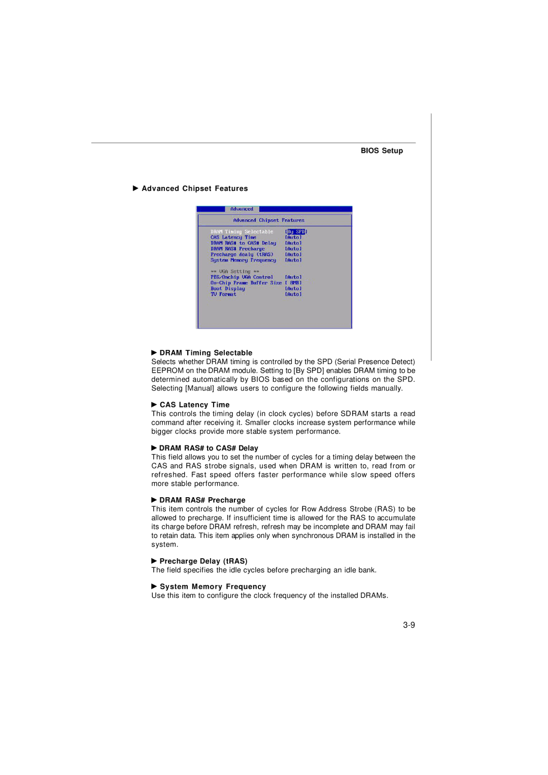
 DRAM Timing Selectable
Selects whether DRAM timing is controlled by the SPD (Serial Presence Detect) EEPROM on the DRAM module. Setting to [By SPD] enables DRAM timing to be determined automatically by BIOS based on the configurations on the SPD. Selecting [Manual] allows users to configure the following fields manually.
 CAS Latency Time
This controls the timing delay (in clock cycles) before SDRAM starts a read command after receiving it. Smaller clocks increase system performance while bigger clocks provide more stable system performance.
 DRAM RAS# to CAS# Delay
This field allows you to set the number of cycles for a timing delay between the CAS and RAS strobe signals, used when DRAM is written to, read from or refreshed. Fast speed offers faster performance while slow speed offers more stable performance.
 DRAM RAS# Precharge
This item controls the number of cycles for Row Address Strobe (RAS) to be allowed to precharge. If insufficient time is allowed for the RAS to accumulate its charge before DRAM refresh, refresh may be incomplete and DRAM may fail to retain data. This item applies only when synchronous DRAM is installed in the system.
 Precharge Delay (tRAS)
The field specifies the idle cycles before precharging an idle bank.
 System Memory Frequency
Use this item to configure the clock frequency of the installed DRAMs.