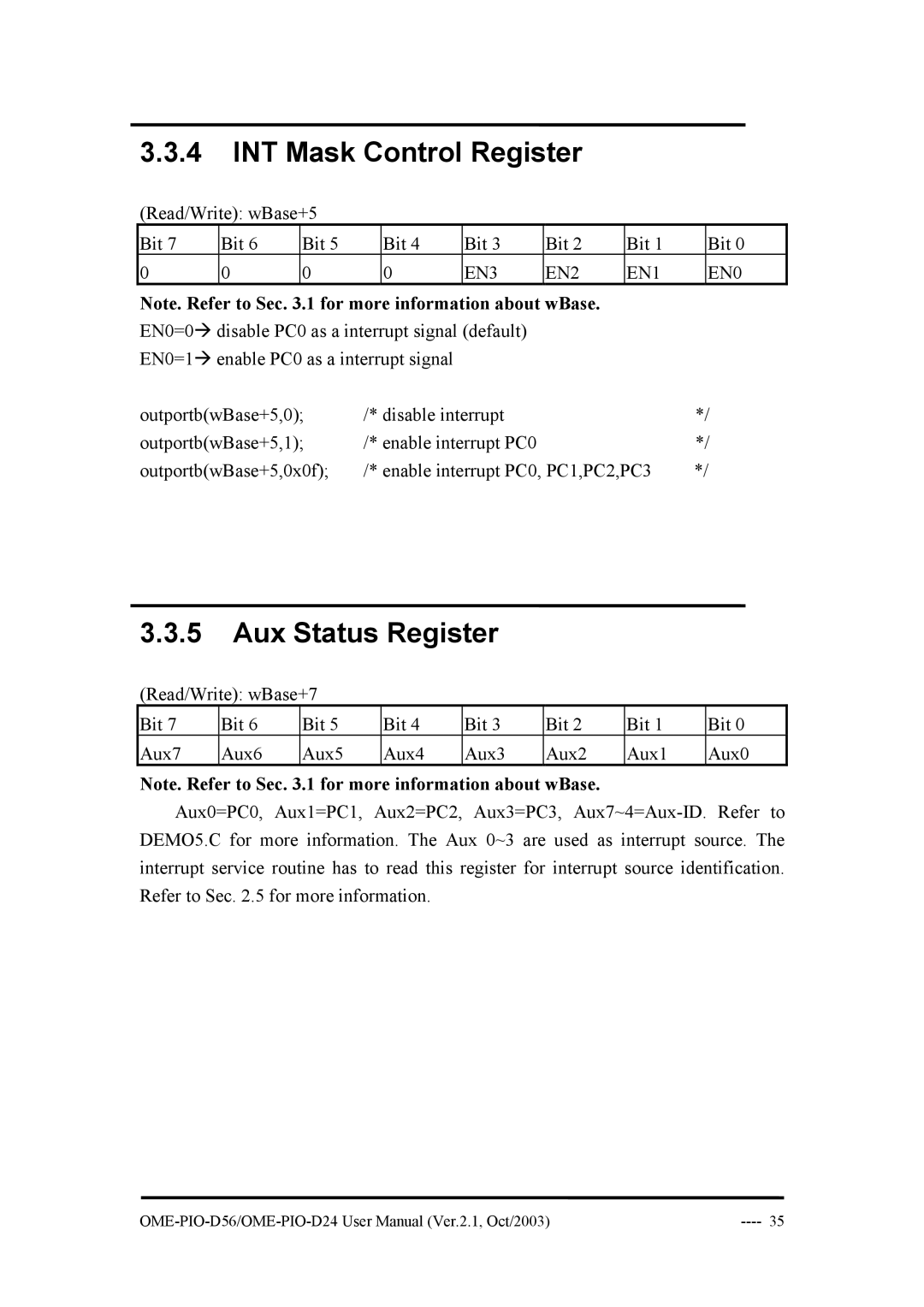
3.3.4INT Mask Control Register
(Read/Write): wBase+5
Bit 7 | Bit 6 | Bit 5 | Bit 4 | Bit 3 | Bit 2 | Bit 1 | Bit 0 |
0 | 0 | 0 | 0 | EN3 | EN2 | EN1 | EN0 |
Note. Refer to Sec. 3.1 for more information about wBase.
EN0=0Æ disable PC0 as a interrupt signal (default)
EN0=1Æ enable PC0 as a interrupt signal
outportb(wBase+5,0); | /* disable interrupt | */ |
outportb(wBase+5,1); | /* enable interrupt PC0 | */ |
outportb(wBase+5,0x0f); | /* enable interrupt PC0, PC1,PC2,PC3 | */ |
3.3.5Aux Status Register
(Read/Write): wBase+7
Bit 7 | Bit 6 | Bit 5 | Bit 4 | Bit 3 | Bit 2 | Bit 1 | Bit 0 |
Aux7 | Aux6 | Aux5 | Aux4 | Aux3 | Aux2 | Aux1 | Aux0 |
Note. Refer to Sec. 3.1 for more information about wBase.
Aux0=PC0, Aux1=PC1, Aux2=PC2, Aux3=PC3,
