Philips Semiconductors | ISP1301 USB OTG Transceiver Eval Kit User’s Guide | |
TABLES |
|
|
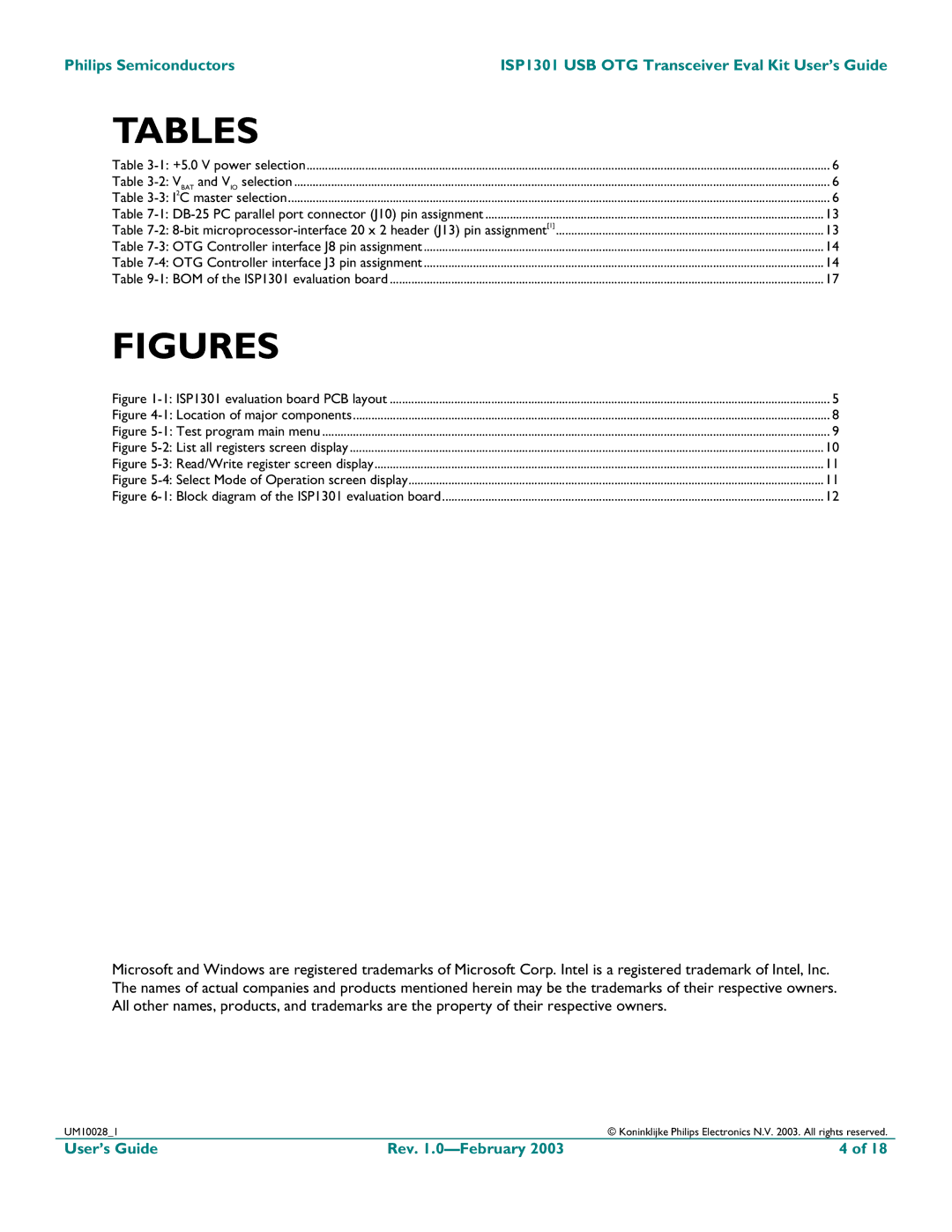
Table | 6 | |
Table | 6 | |
Table | 6 | |
Table | 13 | |
Table | 13 | |
Table | 14 | |
Table | 14 | |
Table | 17 | |
FIGURES |
|
|
Figure | 5 | |
Figure | 8 | |
Figure | 9 | |
Figure | 10 | |
Figure | 11 | |
Figure | 11 | |
Figure | 12 | |
Microsoft and Windows are registered trademarks of Microsoft Corp. Intel is a registered trademark of Intel, Inc. The names of actual companies and products mentioned herein may be the trademarks of their respective owners. All other names, products, and trademarks are the property of their respective owners.
UM10028_1 |
| © Koninklijke Philips Electronics N.V. 2003. All rights reserved. |
User’s Guide | Rev. | 4 of 18 |
