AN.No.G1216B1N000-3D0E
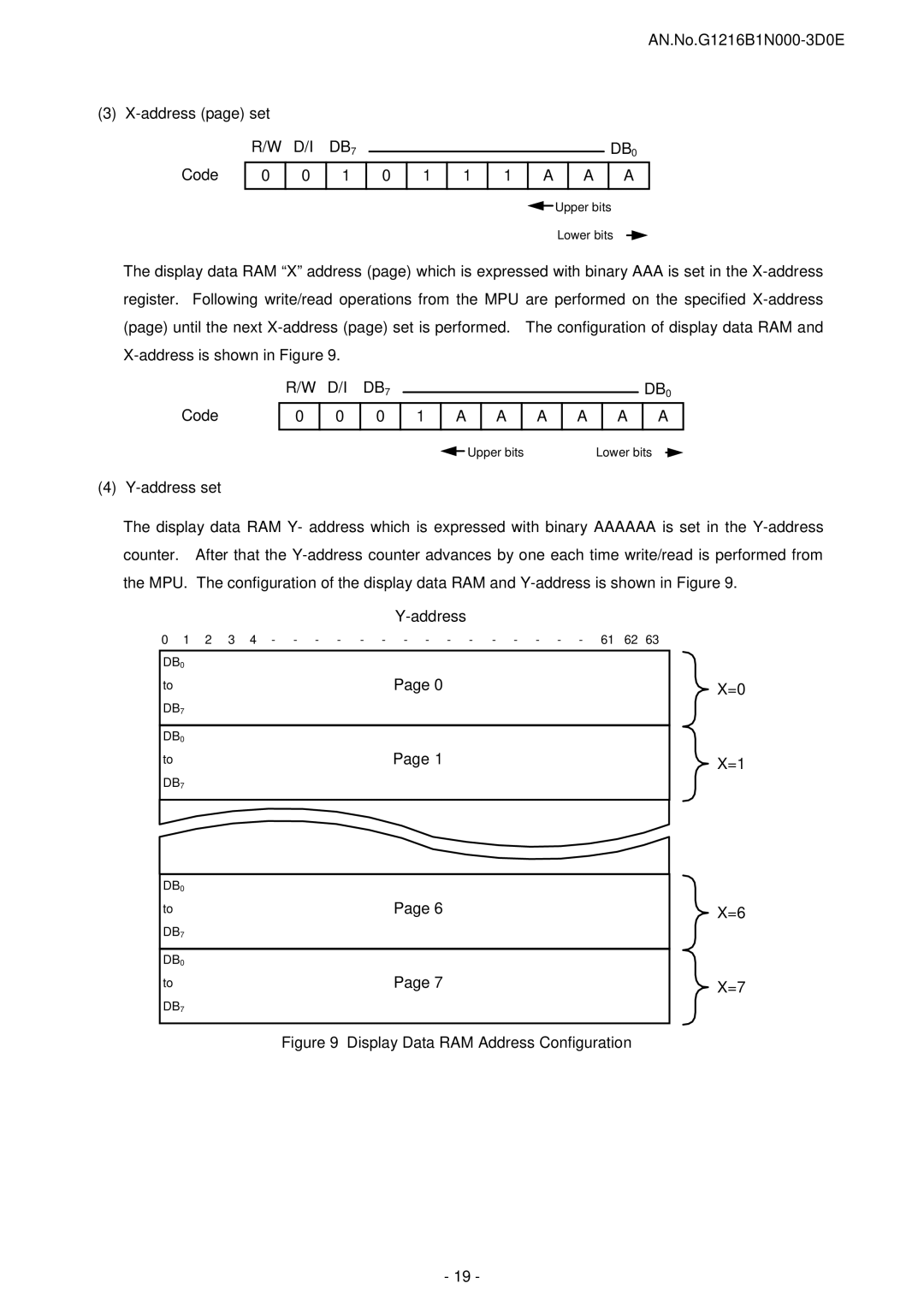
(3) X-address (page) set
Code | R/W | D/I | DB7 |
|
|
|
|
|
|
| DB0 | |
|
|
|
|
|
|
| ||||||
0 | 0 | 1 | 0 | 1 | 1 | 1 | A | A | A | |||
|
|
|
|
|
|
|
|
|
|
|
|
|
![]() Upper bits
Upper bits
Lower bits
The display data RAM “X” address (page) which is expressed with binary AAA is set in the
Code
R/W | D/I | DB7 |
|
|
|
|
|
|
|
| DB0 |
|
|
|
|
|
|
|
| ||||
0 | 0 | 0 | 1 | A | A | A | A | A | A | ||
|
|
|
|
|
|
|
|
|
|
|
|
Upper bits | Lower bits |
(4)
The display data RAM Y- address which is expressed with binary AAAAAA is set in the
| ||
0 1 2 3 4 - - - - | - - - - - - - - - - - 61 62 63 | |
|
|
|
DB0 |
|
|
|
| |
to | Page 0 |
|
DB7 |
|
|
|
| |
|
|
|
DB0 |
|
|
|
| |
to | Page 1 |
|
DB7 |
|
|
|
| |
|
|
|
DB0 |
|
|
|
|
|
to | Page 6 |
|
DB7 |
|
|
|
| |
|
|
|
DB0 |
|
|
|
|
|
to | Page 7 |
|
DB7 |
|
|
|
| |
|
|
|
X=0
X=1
X=6
X=7
Figure 9 Display Data RAM Address Configuration
- 19 -