IC804
Pin No. | Port Name | Function |
|
|
|
1 |
| Driver CH1 negative output |
|
|
|
2 |
| Driver CH1 positive output |
|
|
|
3 |
| Driver CH1 input |
|
|
|
4 |
| Driver CH1 input, gain adjustment pin |
|
|
|
5 | Connect to external transistor base | |
|
|
|
6 |
| Constant voltage output, connects to external transistor collector |
|
|
|
7 | MUTE | Driver mute control input |
|
|
|
8 | GND | GND |
|
|
|
9 |
| Driver CH2 input, gain adjustment pin |
|
|
|
10 |
| Driver CH2 input |
|
|
|
11 |
| Driver CH2 positive output |
|
|
|
12 |
| Driver CH2 negative output |
|
|
|
13 | Substrate GND | Substrate GND |
|
|
|
14* |
| Operational amplifier output |
|
|
|
15* | Operational amplifier input, negative | |
|
|
|
16* | Operational amplifier input, positive | |
|
|
|
17 |
| Driver CH3 negative output |
|
|
|
18 |
| Driver CH3 positive output |
|
|
|
19 |
| Driver CH3 input |
|
|
|
20* |
| Driver CH3 input, gain adjustment pin |
|
|
|
21 | Vcc | Vcc |
|
|
|
22 | Vcc | Vcc |
|
|
|
23 |
| Bias amplifier input |
|
|
|
24 |
| Driver CH4 input, gain adjustment pin |
|
|
|
25 |
| Driver CH4 input |
|
|
|
26 |
| Driver CH4 positive output |
|
|
|
27 |
| Driver CH4 negative output |
|
|
|
28 | Substrate GND | Substrate GND |
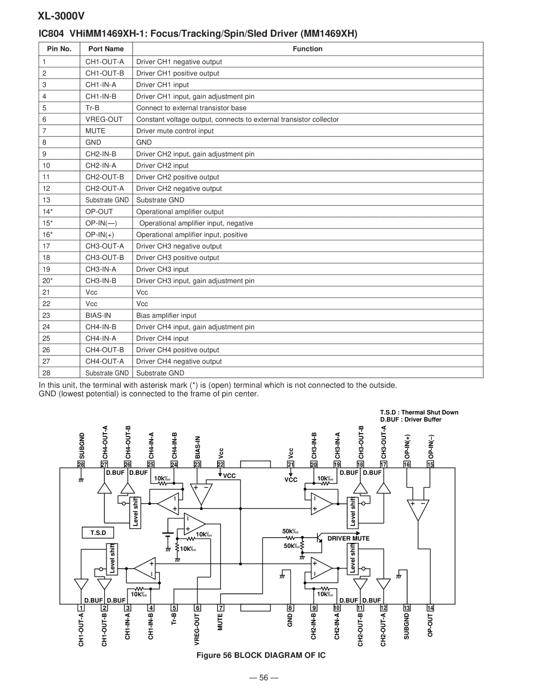
In this unit, the terminal with asterisk mark (*) is (open) terminal which is not connected to the outside. GND (lowest potential) is connected to the frame of pin center.
T.S.D : Thermal Shut Down
D.BUF : Driver Buffer
SUBGND | Vcc | Vcc |
| |||||||||||
28 | 27 | 26 | 25 | 24 | 23 | 22 | 21 | 20 | 19 | 18 | 17 | 16 | 15 | |
| D.BUF | D.BUF |
| 10kΩ |
| VCC |
|
| 10kΩ | D.BUF | D.BUF |
|
| |
|
|
|
|
| VCC |
|
|
|
|
|
| |||
|
|
|
|
|
|
|
|
|
|
|
| |||
|
| Level shift |
|
|
|
| 50kΩ |
|
| Level shift |
|
|
|
|
| T.S.D |
|
|
| 10kΩ |
|
|
|
|
|
|
|
| |
|
|
|
|
|
|
| DRIVER MUTE |
|
|
| ||||
|
|
|
|
|
|
| 50kΩ |
|
|
|
| |||
| Level shift |
|
|
| 10kΩ |
|
|
| Level shift |
|
|
|
| |
|
|
|
|
|
|
|
|
|
|
|
| |||
|
|
|
|
|
|
|
|
|
|
|
|
| ||
|
| 10kΩ |
|
|
|
|
|
| 10kΩ |
|
|
|
|
|
| D.BUF D.BUF |
|
|
|
|
|
| D.BUF | D.BUF |
|
|
| ||
1 | 2 | 3 | 4 | 5 | 6 | 7 | 8 | 9 | 10 | 11 | 12 | 13 | 14 | |
MUTE | GND |
| SUBGND | |||||||||||
Figure 56 BLOCK DIAGRAM OF IC
– 56 –
