SieMo S50037 Data Book PRELIMINARILY
Pin Description
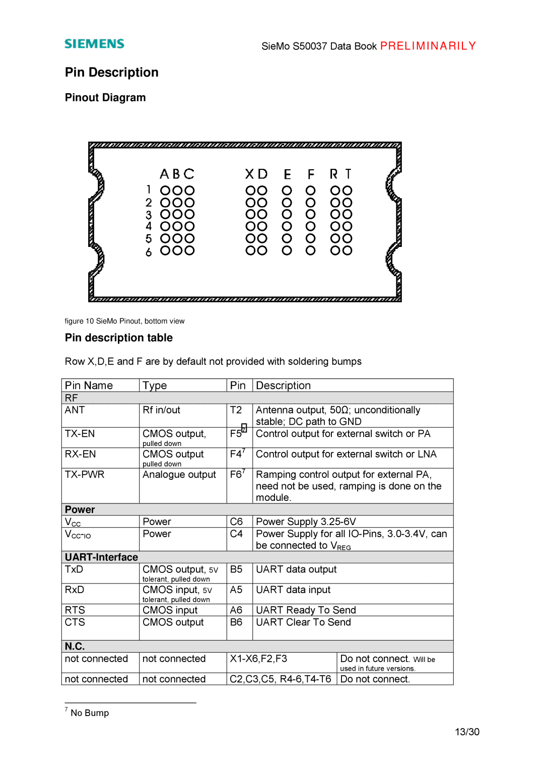
Pinout Diagram
figure 10 SieMo Pinout, bottom view
Pin description table
Row X,D,E and F are by default not provided with soldering bumps
Pin Name
Type
Pin Description
RF
ANT | Rf in/out | T2 | Antenna output, 50Ω; unconditionally | |
|
|
| stable; DC path to GND | |
CMOS output, | F57 | Control output for external switch or PA | ||
| pulled down |
|
|
|
CMOS output | F47 | Control output for external switch or LNA | ||
| pulled down |
|
|
|
| Analogue output | F67 | Ramping control output for external PA, | |
|
|
| need not be used, ramping is done on the | |
|
|
| module. |
|
Power |
|
|
|
|
VCC | Power | C6 | Power Supply | |
Power | C4 | Power Supply for all | ||
|
|
| be connected to VREG | |
|
|
|
| |
TxD | CMOS output, 5V | B5 | UART data output |
|
| tolerant, pulled down |
|
|
|
RxD | CMOS input, 5V | A5 | UART data input |
|
| tolerant, pulled down |
|
|
|
RTS | CMOS input | A6 | UART Ready To Send | |
CTS | CMOS output | B6 | UART Clear To Send | |
|
|
|
|
|
N.C. |
|
|
|
|
not connected | not connected | Do not connect. Will be | ||
|
|
|
| used in future versions. |
not connected | not connected | C2,C3,C5, | Do not connect. | |
7No Bump
13/30
