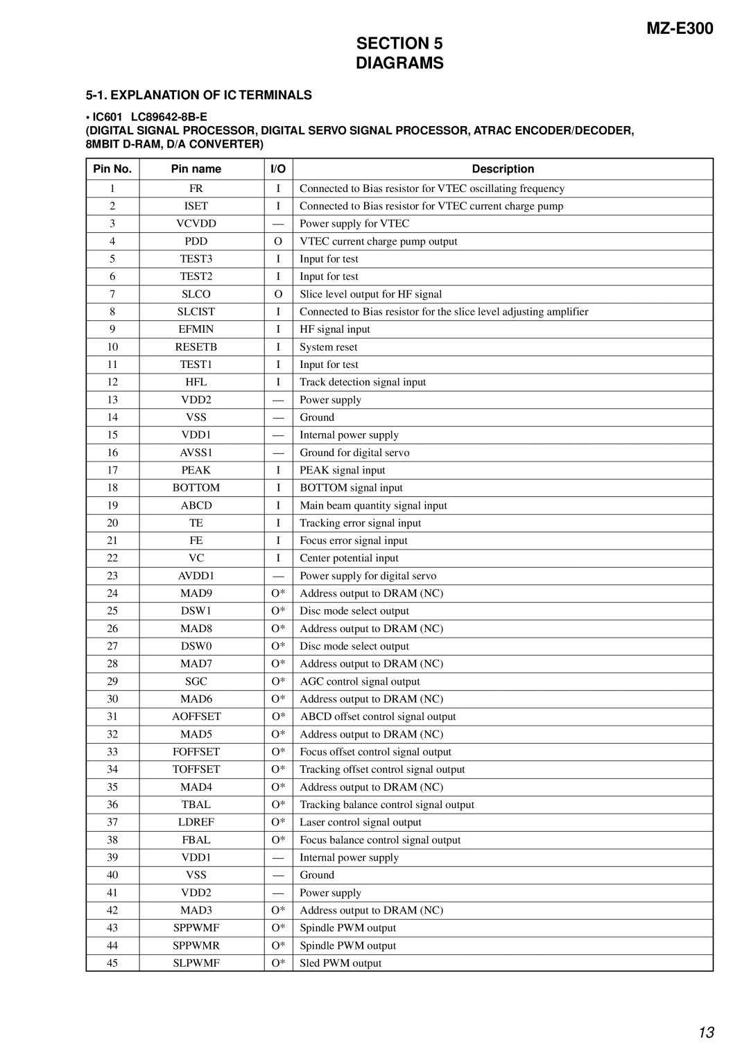
MZ-E300
SECTION 5
DIAGRAMS
5-1. EXPLANATION OF IC TERMINALS
• IC601 LC89642-8B-E
(DIGITAL SIGNAL PROCESSOR, DIGITAL SERVO SIGNAL PROCESSOR, ATRAC ENCODER/DECODER, 8MBIT
Pin No. | Pin name | I/O | Description |
|
|
|
|
1 | FR | I | Connected to Bias resistor for VTEC oscillating frequency |
|
|
|
|
2 | ISET | I | Connected to Bias resistor for VTEC current charge pump |
|
|
|
|
3 | VCVDD | — | Power supply for VTEC |
|
|
|
|
4 | PDD | O | VTEC current charge pump output |
|
|
|
|
5 | TEST3 | I | Input for test |
|
|
|
|
6 | TEST2 | I | Input for test |
|
|
|
|
7 | SLCO | O | Slice level output for HF signal |
|
|
|
|
8 | SLCIST | I | Connected to Bias resistor for the slice level adjusting amplifier |
|
|
|
|
9 | EFMIN | I | HF signal input |
|
|
|
|
10 | RESETB | I | System reset |
|
|
|
|
11 | TEST1 | I | Input for test |
|
|
|
|
12 | HFL | I | Track detection signal input |
|
|
|
|
13 | VDD2 | — | Power supply |
|
|
|
|
14 | VSS | — | Ground |
|
|
|
|
15 | VDD1 | — | Internal power supply |
|
|
|
|
16 | AVSS1 | — | Ground for digital servo |
|
|
|
|
17 | PEAK | I | PEAK signal input |
|
|
|
|
18 | BOTTOM | I | BOTTOM signal input |
|
|
|
|
19 | ABCD | I | Main beam quantity signal input |
|
|
|
|
20 | TE | I | Tracking error signal input |
|
|
|
|
21 | FE | I | Focus error signal input |
|
|
|
|
22 | VC | I | Center potential input |
|
|
|
|
23 | AVDD1 | — | Power supply for digital servo |
|
|
|
|
24 | MAD9 | O* | Address output to DRAM (NC) |
|
|
|
|
25 | DSW1 | O* | Disc mode select output |
|
|
|
|
26 | MAD8 | O* | Address output to DRAM (NC) |
|
|
|
|
27 | DSW0 | O* | Disc mode select output |
|
|
|
|
28 | MAD7 | O* | Address output to DRAM (NC) |
|
|
|
|
29 | SGC | O* | AGC control signal output |
|
|
|
|
30 | MAD6 | O* | Address output to DRAM (NC) |
|
|
|
|
31 | AOFFSET | O* | ABCD offset control signal output |
|
|
|
|
32 | MAD5 | O* | Address output to DRAM (NC) |
|
|
|
|
33 | FOFFSET | O* | Focus offset control signal output |
|
|
|
|
34 | TOFFSET | O* | Tracking offset control signal output |
|
|
|
|
35 | MAD4 | O* | Address output to DRAM (NC) |
|
|
|
|
36 | TBAL | O* | Tracking balance control signal output |
|
|
|
|
37 | LDREF | O* | Laser control signal output |
|
|
|
|
38 | FBAL | O* | Focus balance control signal output |
|
|
|
|
39 | VDD1 | — | Internal power supply |
|
|
|
|
40 | VSS | — | Ground |
|
|
|
|
41 | VDD2 | — | Power supply |
|
|
|
|
42 | MAD3 | O* | Address output to DRAM (NC) |
|
|
|
|
43 | SPPWMF | O* | Spindle PWM output |
|
|
|
|
44 | SPPWMR | O* | Spindle PWM output |
|
|
|
|
45 | SLPWMF | O* | Sled PWM output |
13