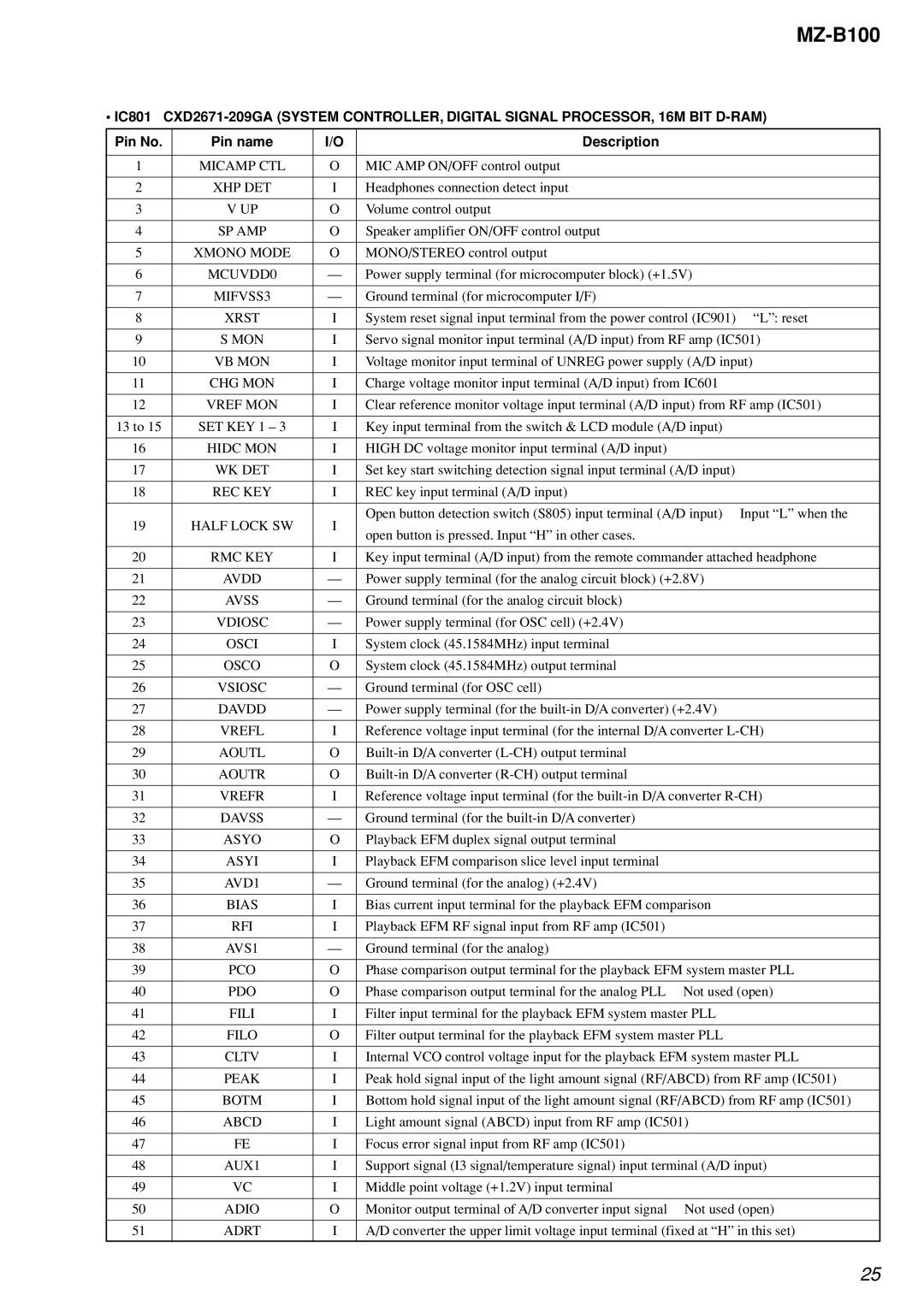
MZ-B100 specifications
The Sony MZ-B100 is a remarkable mini disc player that stands out for its innovative features and technologies, catering to music enthusiasts and professionals alike. Released in the early 2000s, it represents a significant advancement in portable audio technology, combining convenience with high-quality sound reproduction.One of the key features of the MZ-B100 is its lightweight and compact design, making it highly portable. It allows users to enjoy their favorite music on the go without being burdened by heavy equipment. The device supports the MiniDisc format, which was widely appreciated for its ability to store high-quality audio while offering the flexibility of recording and erasing tracks easily.
The MZ-B100 boasts a range of audio recording capabilities. With its built-in microphone, users can easily capture live performances, meetings, or personal notes. The player features a record timer, which enables timed recordings, an invaluable tool for those who need to capture audio at specific moments. Additionally, the unit supports various recording modes, including LP2 and LP4, allowing users to choose between quality and capacity.
In terms of sound quality, the MZ-B100 employs Sony's ATRAC compression technology. This technology preserves the audio quality while minimizing file sizes, enabling users to store more tracks on a single MiniDisc. The device also includes a digital pitch control feature, which allows users to adjust the playback speed without altering the pitch. This is particularly useful for musicians practicing with recorded accompaniments.
Another standout characteristic of the MZ-B100 is its battery life. Equipped with rechargeable batteries, the device provides extended playback time, ensuring that users can enjoy hours of music without frequent recharges. The user interface is intuitive, featuring a clear display that makes navigation through tracks and playlists seamless.
Connectivity is another important aspect of the MZ-B100. It includes various input and output options, allowing users to connect the player to external audio systems, enabling them to play music through larger speakers or transfer recordings to a computer.
Overall, the Sony MZ-B100 mini disc player is a well-rounded device packed with advanced features aimed at enhancing the listening experience. Its portability, sound quality, and intuitive functionality make it a noteworthy choice for anyone seeking a reliable audio recording and playback solution. The MZ-B100 remains a testament to Sony's commitment to innovation in the world of personal audio technology.
