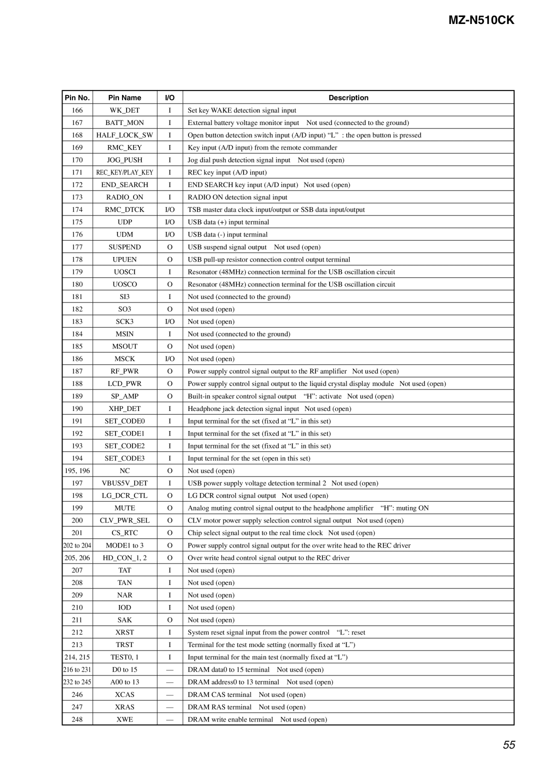
MZ-N510CK specifications
The Sony MZ-N510CK is a sophisticated mini-disc player that epitomizes the blend of portability and high-fidelity audio technology. Introduced in the early 2000s, this device became a favorite among audiophiles and casual listeners alike due to its compact design and impressive features. One of the standout characteristics of the MZ-N510CK is its ability to record in both SP and LP mode. SP mode offers crisp, CD-quality sound, while LP mode allows users to store more audio tracks onto a single disc, providing flexibility for users who prioritize capacity over audio fidelity.The MZ-N510CK is equipped with Sony’s ATRAC (Adaptive Transform Acoustic Coding) technology. This lossy compression algorithm was designed to reduce the size of audio files without significantly compromising sound quality. With ATRAC, users can enjoy extended playtime on their mini-discs while maintaining an enjoyable listening experience. This makes the device particularly useful for long trips or extended listening sessions.
Another key feature of the MZ-N510CK is its superb battery life. Sporting an efficient power management system, the player can provide several hours of playback on just a single charge. This is especially advantageous for users who frequently travel, as it minimizes downtime waiting for the device to recharge.
The MZ-N510CK also boasts a sleek, user-friendly interface that enhances its overall usability. The easy-to-read LCD screen allows users to navigate through tracks seamlessly. Additionally, this model comes with a skip-free playback feature, which is particularly helpful during activities like jogging or walking, where bumps and jostles might typically disturb audio playback.
For connectivity, the MZ-N510CK includes a USB port, facilitating easy transfer of music files from a computer to the mini-disc. This connectivity feature was relatively advanced for the time, making the device more versatile in an era where digital music was rapidly on the rise.
In essence, the Sony MZ-N510CK presents an impressive package of features: high-quality audio recording options, cutting-edge compression technology, long battery life, a convenient interface, and strong connectivity options. Its combination of portability and performance makes it a remarkable device that continues to be appreciated by those who value high-quality sound in a compact format.
