MZ-NH700/NHF800

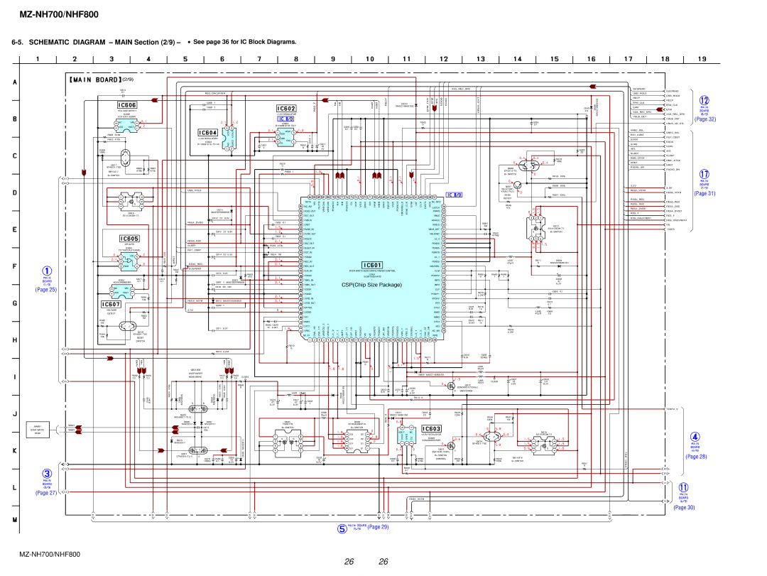
6-5. SCHEMATIC DIAGRAM – MAIN Section (2/9) – See page 36 for IC Block Diagrams.

(Page 25)

(2/9)


C673


0.1


REG_DACVREFH


C668

1


C669

1


VOLTAGE DETECT


IC606


XC61CN1702NR


NC


VIN


VSS

VOUT


R663

220k


VDD

VOUT


R662

470k


+1.2V REGULATOR


GND


IC604


NC


R1180Q121C-TR-FA


R659


100k


-1


-2


Q617


XP4601-TXE


R660

R661


Q616,617


470k

470k


B+ SWITCH


A1


A2


USB_HOLD


S


D614


Q616


MA2SD32008S0


SI1410EDH-T1


C612

22

6.3V


REG4_DVDD


C613

22

6.3V


REG5_OSC


OR GATE


SLEEP


IC605


TC7S32LFU(TE85R)


RST_CONT


0


C614

22

6.3V


VCC


922 67R

XRST


REG5_REG


GND


SUSPEND


R647


1M


C675

0.01


R653


C677

C671


22k


IC607


D601


0.1


0.1


C607

1


XC61CN8902NR


MA2SD32008S0


NC

VIN


C616

22

10V


VSS

VOUT


R685


10k


REG5_VSTB

D613

MA2SD32008S0


C609

1


VOLTAGE


3.3V


DETECT


R683


R682


1M


1M


-1

-2


C611

0.01


Q618


R684


XP4601-TXE


10k


RESET


SWITCH


A3


R612

2.2M


A4


HAB

HA


HB

HBB


Q601,602


R622


R620


OVER WRITE


R621


R623


HEAD DRIVE


CL604


2.2


2.2


2.2


2.2


A5


FREG

+1.2V REGULATOR


IC602


R1160N121B-TR-F


VOUT


VDD


1


GND


9

ECO


1


6C

CE


C601

R652

C621

10

1

0

4V


R678


0


R608

1


OUTA


OUTB

VRECIN

VRECIN


HOLD_OUTVG


NC_AI2


RST_OUT


PVBUS


C602

0.1


CRST


DVDD_IN


DVDD_OUT


C604

0.1


HOLDC


R645

470k

OSC_OUT


SLEEP_IN


R654

1M

RST_IN


PGND2


REG_IN


REG_OUT


SUS_IN


PGND2


TSBV_IN


TSBV_OUT


VD33R


PGND1


VSTB_IN


VSTB_OUT


BATSEL


V33RO


RF1


INM1


2VRECQ

1VRECQ

R605 C620

DTC1

1BDW

1TDW

1k

0.047

NC_A1

VREC

R670

0

HA

HB

HAB

HBB

RECP

D610

CLKEFM

EFM

4FS

SDO0

MA2Z748001S0

R643

0

C625 C630

0.10.1

PGND2

HA

HB

PGND4

CL

VCP

VG2

GND

CH

HAB

HBB

GND

RECP

VG3

PGND4

VBUSSEL2

CLKEFM

EFM

VIF

CLK

DATA

SCK

NC_M12

LATCH

XWKO

VBUS


WAKEC


V33UO


VBUS_DET


VBUSREF


L5_2


PGND5


PGND5


POWFB


L5_1


PGND5


VBUSSEL


OVER WRITE HEAD DRIVE,POWER CONTROL


CLM


IC601


POWP2


SC901585VAR2


*


INP3


CSP(Chip Size Package)


INP2


CLP


POWP1


VPDRV


RF2


DTC2


INM2


INM3


DTC3


1TUP

1BUP


PGND1


PGND3

PGND1

3BUP

VREFIN

PGND3

PGND3


33USEL


3TDW

3BDW


RF3

2L1

1L1

INP1

GND


1V30

2V30

1L3

2L3


NC_M1

VC

VC


V3FB


R671


R680


0


0


D603


MA2Z748001S0


XCS_REC_DRV

SCK0

DETVBUS

Q608

XP4314-TX

B+ SWITCH

Q607 2SC4738F- Y/GR(TPL3)

DC IN

DETECT

R646

47k

R681

1M

C644

4700p

L607

47H

R665

R649

R648

0

1

1

R675

2.2M

C641 R616

0.011k

C642 R617

0.047 1k

R629

2.2M

C645C638

0.012200p

L605

22H

C637

L603 CL65810

10H

C636

0.1

R618

100k

-1

-2

R619 100k

R609 100k

R601 220k

Q611

SI1410EDH-T1

S

B+ SWITCH

R677D604

0MA22D2800LS0

C658

47

6.3V

C666 4.7

C672

4.7

L608 R664

47H 2.2

C653

10

C643

2.2

R628

22


SUSPEND


SUSPEND


USB_HOLD


USB_HOLD

0S

RECP

RECP

09D6 001Z748

EFM_CLK

EFM_CLK

EFM

EFM

2

XCS_REC_DRV

A

XCS_REC_DRV

M

VBUS_DET


VBUS_DET

(Page 32)

VBUS_VB_CTL

VREC_SEL


VREC_SEL


RST_CONT


RST_CONT


SDO0


SDO0


SCK0


SCK0


4FS


4FS


SLEEP


SLEEP


RMC_DTCK


RMC_DTCK


XRST


XRST


RADIO_ON


RADIO_ON


3.3V

3.3V

REG5_VSTB

REG5_VSTB

(Page 31)

REG5_REG

REG5_REG

REG5_OSC

REG5_OSC

REG4_DVDD

REG4_DVDD

REG_F

REG_F

REG_DACVREFH

REG_DACVREFH

VB

DDC3

6.3V6.3V

Q612

HR601

OVER WRITE


47


47

0


047.0

64 704 6C . 0

426 R

50 30DS 6D 2A M

S

S

860 30DS D 2 AM

562 R

846 C


2-

1-


Q602


MCH6617-TL-E


D606


D607


W601


MA22D17


MA22D17


C674


W602


33p


L601


C622

C627

C628

47

47

1

6.3V

6.3V


L606

10H

Q603

TS8K1TB

B+ SWITCH

0


C635


S1

C633

C634


0

0.01

1

47


026 084Z7 D


6.3V


R673

0

2AM


0

D611


C661


MA2Z748001S0


2.2

Q609

536 R


NTHD4508NTIG


B+ SWITCH

SSM3K01F(TE85L)

S SWITCHING

R638

220k

R640R641

220k1M

HEAD

(Page 27)

D615


17D

MA22D17


2-

1-


22AM

Q601


16

CPH5614-TL-E

S


6D


C676

C649

C650


10


1000p

0.1


6.3V

C1


C2


C3

SS

C652

10

6.3V

D2

G2

VOUT

NC

+3.2V REGULATOR


Q615

VDD

GND

CE

-1

-2

SI1410EDH-T1

D2

S2


IC603


XC6209B322MR

Q614


D1

G1


XP4601-TXE


D1

S1


Q613

S


S


2SK1830-TE85L


B+ SWITCH


Q614,615


C660


R636

CONTROL

R639

R642


0.1


470k


1M

100k

B+ SWITCH


R650


4.7


REG5_VSTB

1E

E2

E3

E4

5E

E6

E7

8E

9E

01E

11E

(Page 29)

R657

0

TERRA_V

SEL

(Page 28)

VREC


D2

D1

F1

F2

(Page 30)

13E

MZ-NH700/NHF800

26 26

Page 26
Image 26
Sony NHF800 service manual Schematic Diagram Main /9 See page 36 for IC Block Diagrams, Gnd

NHF800 specifications

The Sony NHF800 is a remarkable addition to Sony's range of high-fidelity audio devices, designed to elevate the listening experience for audiophiles and casual listeners alike. Blending cutting-edge technology with user-friendly features, the NHF800 stands out as a versatile and powerful audio solution.

At the heart of the NHF800 is its advanced audio circuitry, which employs high-resolution audio technology. This ensures that music playback is not only accurate but also retains the depth and richness of the original recordings. Supporting various audio formats, including DSD, PCM, and even compressed formats, this device caters to diverse musical tastes while maintaining superior sound quality.

One of the standout features of the Sony NHF800 is its compatibility with both wired and wireless connections. With Bluetooth capabilities, users can stream music effortlessly from smartphones, tablets, or computers, while the high-resolution audio ensures that streamed content does not compromise on quality. Additionally, the device is equipped with Wi-Fi support, allowing for easy access to streaming services and internet radio, further broadening the audio horizons for users.

The NHF800 also boasts a built-in DAC (Digital-to-Analog Converter) that promotes enhanced audio performance. This DAC converts digital signals into analog with precision, resulting in a cleaner, more detailed sound output. The device supports a wide dynamic range, allowing listeners to experience their music as intended by the artists.

Moreover, the NHF800 features an intuitive user interface that simplifies navigation through music libraries and settings. The color display provides clear visuals, making it easy to browse albums, playlists, and streaming options. The device's ergonomic design ensures that it is not only visually appealing but also comfortable to use, whether at home or on the go.

Further enhancing the listening experience, the device incorporates noise-canceling technologies, allowing users to enjoy their music without external interruptions. This feature is particularly beneficial for users in noisy environments, such as public transport or busy urban settings.

In summary, the Sony NHF800 is a well-rounded high-fidelity audio device that merges advanced technology with usability. Its high-resolution audio capability, extensive connectivity options, and user-friendly design make it an excellent choice for anyone looking to elevate their listening experience. Whether at home or out and about, the NHF800 ensures that every note resonates with clarity and detail, making music come alive like never before.