NWZ-A826/A826K/A828/A828K/A829
MAIN BOARD IC601
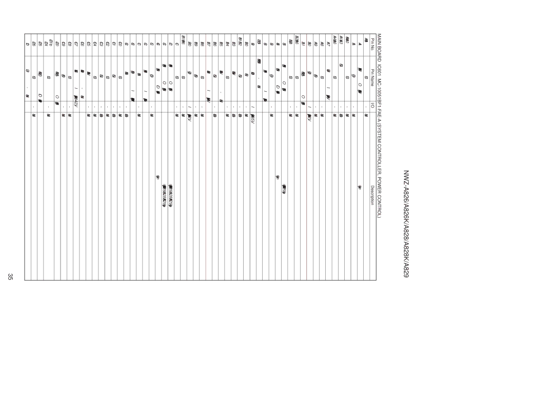
Pin No. | Pin Name | I/O | Description | |
A1 to A3 | NC | - | Not used | |
A4 | NAND_WEZ | O | Write enable signal output to the NAND flash memory | |
A5 | IO_B | - | Not used | |
A6 to A10 | NC | - | Not used | |
A11 to A13 | GND | - | Ground terminal | |
A14 to A16 | NC | - | Not used | |
A17 | VCCVBUS | I | Power supply input terminal (+5V) | |
A18 | NC | - | Not used | |
A19 | IO_A | - | Not used | |
A20 | VDD_L0 | I | Power supply input terminal (+1.2V) | |
A21 | AB0_A8 | O | Address signal output to the USB controller | |
A22 to A26 | NC | - | Not used | |
B1, B2 | NC | - | Not used | |
B3 | NAND_CEZ2 | O | Chip enable signal output to the NAND flash memory | |
B4 | NAND_DA0 | I/O | ||
B5 | IO_B | - | Not used | |
B6 | KEY_AD1 | I | Key input terminal (A/D input) | |
B7, B8 | ADIN6, ADIN8 | - | Not used | |
B9 | ADVCC | I | Power supply input terminal (+2.85V) | |
B10 | CPEN | - | Not used | |
B11, B12 | GND | - | Ground terminal | |
B13 | SWGND | - | Ground terminal | |
B14 | NC | - | Not used | |
B15 | SWADP2 | - | Not used | |
B16 | GND | - | Ground terminal | |
B17 | VCCADP | I | Power supply input terminal (+5V) | |
B18 | NC | - | Not used | |
B19 | IO_A | - | Not used | |
B20 | VDD_L0 | I | Power supply input terminal (+1.2V) | |
B21 to B26 | NC | - | Not used | |
C1 | NC | - | Not used | |
C2 | NAND_CEZ1 | O | Chip enable signal output to the NAND flash memory | |
C3 | NAND_CEZ3 | O | Chip enable signal output to the NAND flash memory | |
C4 | NAND_DA1 | I/O | ||
C5 | IO_B | - | Not used | |
C6 | KEY_AD0 | I | Key input terminal (A/D input) | |
C7 | ADIN5 | - | Not used | |
C8 | CRD_AD | I | A/D value detection signal input from the | |
C9 | ADGND | - | Ground terminal | |
C10 | NC | - | Not used | |
C11 | GND | - | Ground terminal | |
C12 | NC | - | Not used | |
C13 | GND | - | Ground terminal | |
C14 | NC | - | Not used | |
C15 | SWADP | - | Not used | |
C16 | CAPVBDL | - | Not used | |
C17 | VCCVBAT | I | Power supply input terminal (+2.3 - 4.2V) | |
C18 | NC | - | Not used | |
C19 | IO_A | - | Not used | |
C20 | AB0_A5 | O | Address signal output to the USB controller | |
C21 to | NC | - | Not used | |
C24 | ||||
|
|
| ||
C25 | AB0_D1 | I/O | ||
C26 | NC | - | Not used | |
D1 | IDPULLUP | - | Not used |
35