NWZ-A826/A826K/A828/A828K/A829
THIS NOTE IS COMMON FOR PRINTED WIRING BOARDS AND SCHEMATIC DIAGRAMS. (In addition to this, the necessary note is printed in each block.)
For Printed Wiring Boards.
Note:
•X : Parts extracted from the component side.
•![]() : Pattern from the side which enables seeing. (The other layers' patterns are not indicated.)
: Pattern from the side which enables seeing. (The other layers' patterns are not indicated.)
Caution: |
|
Parts face side: | Parts on the parts face side seen from |
(SIDE A) | the pattern face are indicated. |
Pattern face side: | Parts on the pattern face side seen from |
(SIDE B) | the parts face are indicated. |
•MAIN and SW boards are
•Indication of transistor.
C |
|
Q | These are omitted. |
BE
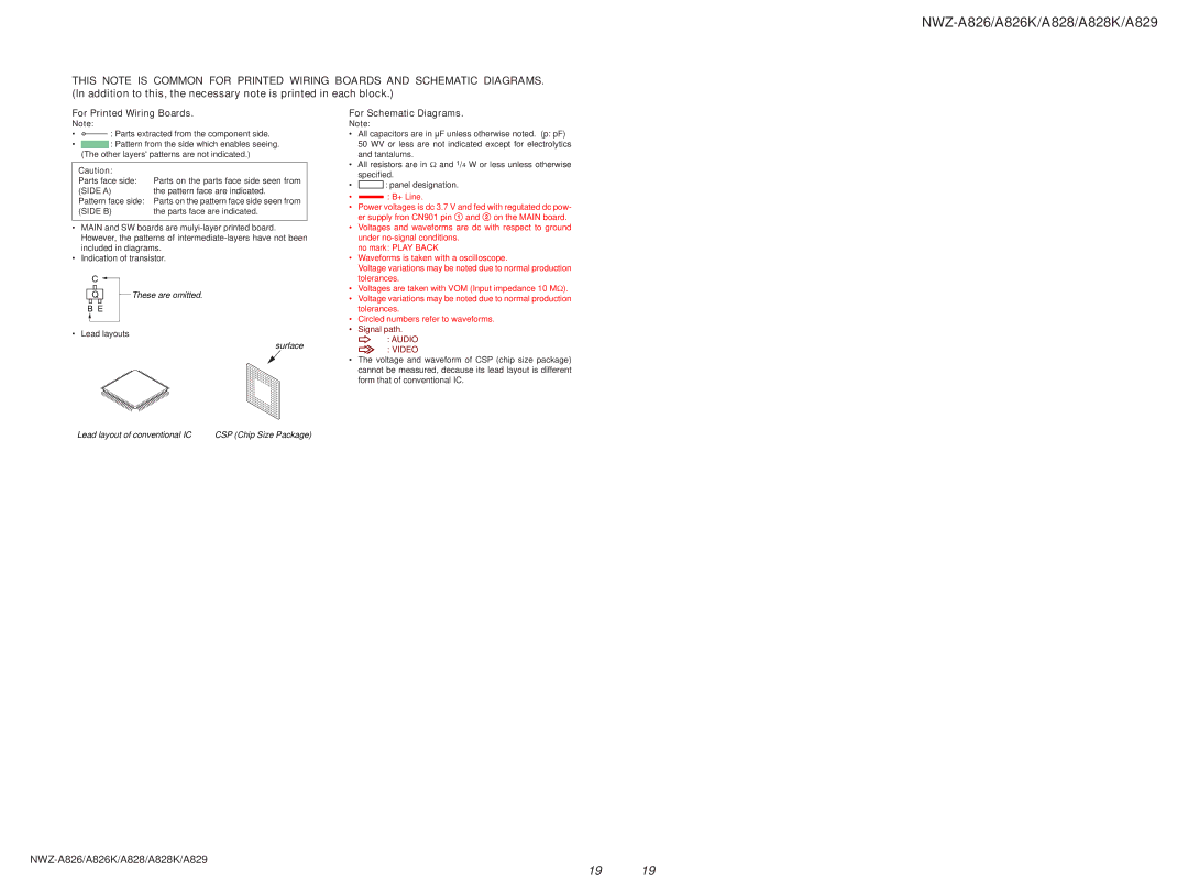
•Lead layouts
surface
For Schematic Diagrams.
Note:
•All capacitors are in μF unless otherwise noted. (p: pF) 50 WV or less are not indicated except for electrolytics and tantalums.
•All resistors are in Ω and 1/4 W or less unless otherwise specified.
•C: panel designation.
•A : B+ Line.
•Power voltages is dc 3.7 V and fed with regutated dc pow- er supply fron CN901 pin 1 and 2 on the MAIN board.
•Voltages and waveforms are dc with respect to ground under
no mark: PLAY BACK
•Waveforms is taken with a oscilloscope.
Voltage variations may be noted due to normal production tolerances.
•Voltages are taken with VOM (Input impedance 10 MΩ).
•Voltage variations may be noted due to normal production tolerances.
•Circled numbers refer to waveforms.
•Signal path.
F : AUDIO
L : VIDEO
•The voltage and waveform of CSP (chip size package) cannot be measured, decause its lead layout is different form that of conventional IC.
Lead layout of conventional IC | CSP (Chip Size Package) |
19 19