Sun Microsystems, Inc. | Netra 240 Server Architecture P9 |
•Dual DTLBs with programmable page size support offer performance improvements for floating point-intensive applications.
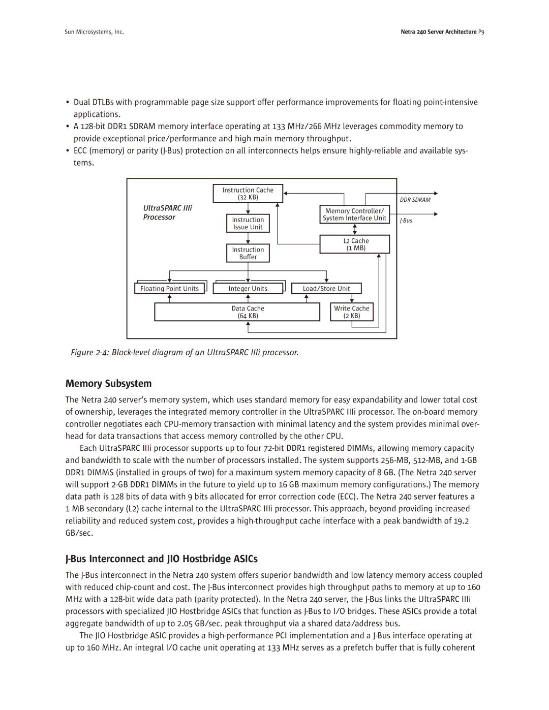
•A 128-bit DDR1 SDRAM memory interface operating at 133 MHz/266 MHz leverages commodity memory to provide exceptional price/performance and high main memory throughput.
•ECC (memory) or parity (J-Bus) protection on all interconnects helps ensure highly-reliable and available sys- tems.
| Instruction Cache | | |
| (32 KB) | | DDR SDRAM |
| | |
UltraSPARC IIIi | | Memory Controller/ | |
Processor | | |
Instruction | System Interface Unit | J-Bus |
| Issue Unit | | |
| | L2 Cache | |
| Instruction | (1 MB) | |
| Buffer | | |
Floating Point Units | Integer Units | Load/Store Unit | |
| Data Cache | Write Cache | |
| (64 KB) | (2 KB) | |
Figure 2-4: Block-level diagram of an UltraSPARC IIIi processor.
Memory Subsystem
The Netra 240 server’s memory system, which uses standard memory for easy expandability and lower total cost of ownership, leverages the integrated memory controller in the UltraSPARC IIIi processor. The on-board memory controller negotiates each CPU-memory transaction with minimal latency and the system provides minimal over- head for data transactions that access memory controlled by the other CPU.
Each UltraSPARC IIIi processor supports up to four 72-bit DDR1 registered DIMMs, allowing memory capacity and bandwidth to scale with the number of processors installed. The system supports 256-MB, 512-MB, and 1-GB DDR1 DIMMS (installed in groups of two) for a maximum system memory capacity of 8 GB. (The Netra 240 server will support 2-GB DDR1 DIMMs in the future to yield up to 16 GB maximum memory configurations.) The memory data path is 128 bits of data with 9 bits allocated for error correction code (ECC). The Netra 240 server features a 1 MB secondary (L2) cache internal to the UltraSPARC IIIi processor. This approach, beyond providing increased reliability and reduced system cost, provides a high-throughput cache interface with a peak bandwidth of 19.2 GB/sec.
J-Bus Interconnect and JIO Hostbridge ASICs
The J-Bus interconnect in the Netra 240 system offers superior bandwidth and low latency memory access coupled with reduced chip-count and cost. The J-Bus interconnect provides high throughput paths to memory at up to 160 MHz with a 128-bit wide data path (parity protected). In the Netra 240 server, the J-Bus links the UltraSPARC IIIi processors with specialized JIO Hostbridge ASICs that function as J-Bus to I/O bridges. These ASICs provide a total aggregate bandwidth of up to 2.05 GB/sec. peak throughput via a shared data/address bus.
The JIO Hostbridge ASIC provides a high-performance PCI implementation and a J-Bus interface operating at up to 160 MHz. An integral I/O cache unit operating at 133 MHz serves as a prefetch buffer that is fully coherent

