
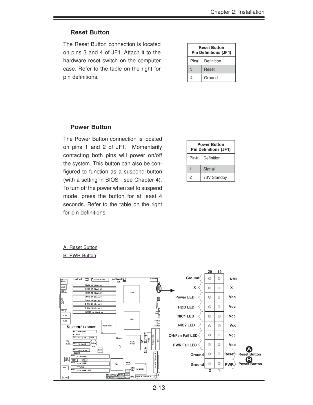
X7DB8, X7DBE specifications
Super Micro Computer, a global leader in high-performance server and storage solutions, has developed a range of advanced server motherboards, among which the X7DBE and X7DB8 stand out for their robust performance and versatility. Designed for data-intensive applications, these motherboards cater to various markets, including cloud computing, enterprise data centers, and video surveillance.The X7DBE motherboards are built on the Intel 5000 series chipset and support dual Intel Xeon processors, which provide exceptional processing power for demanding applications. With a maximum memory capacity of 64GB, these motherboards cater to memory-intensive workloads, making them ideal for virtualization and database applications. The X7DBE supports both ECC (Error-Correcting Code) and non-ECC memory, enhancing system reliability and data integrity.
In terms of storage, the X7DBE is equipped with multiple 3.5-inch SATA hard drive bays that allow for substantial data storage capabilities. Additionally, it includes integrated RAID support, enabling users to configure their storage environment for optimal performance and redundancy. The advanced thermal management technology ensures efficient cooling, promoting system stability and longevity even under heavy workloads.
The X7DB8, on the other hand, takes performance a notch higher by providing support for the latest Intel processors and offering enhanced features geared toward high-performance computing. Like the X7DBE, it supports dual processors but extends capability for larger memory configurations, allowing up to 128GB of DDR2 memory. This flexibility makes the X7DB8 an excellent choice for mission-critical applications requiring immense processing power.
Both motherboards come equipped with multiple PCI Express slots, enabling the installation of add-on cards for tasks such as enhanced graphics, additional network interfaces, or dedicated storage controllers, thus providing scalability to meet the growing demands of modern applications. Network connectivity is robust, with several Gigabit Ethernet ports ensuring high-speed data transfer.
In conclusion, Super Micro's X7DBE and X7DB8 motherboards exemplify the perfect blend of performance, scalability, and reliability. With their support for advanced technologies and their ability to handle high workloads, they are ideal solutions for businesses seeking to optimize their server infrastructure. As technology continues to evolve, these motherboards remain pertinent, providing a solid foundation for various applications and future advancements.