
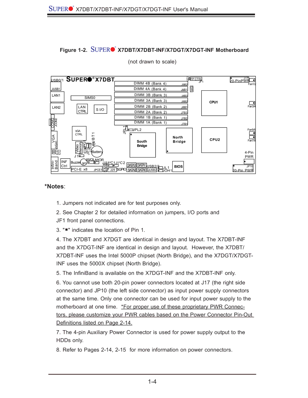
X7DBT, X7DBT-INF, XDGT, X7DGT-INF specifications
Super Micro Computer, a leader in high-performance computing solutions, offers a diverse range of server motherboards tailored for various business needs. Among these, the Supermicro X7DGT-INF, X7DGT, X7DBT-INF, and X7DBT stand out for their robust architectures and advanced features.The Supermicro X7DGT-INF motherboard is designed for dual processor systems utilizing Intel's Xeon processors. It supports up to 64GB of DDR2 memory, providing significant flexibility for memory-intensive applications. The X7DGT-INF features six SATA ports, enabling efficient data storage solutions with RAID configurations. Additionally, it offers integrated IPMI (Intelligent Platform Management Interface) functionality, which allows remote management of the motherboard, enhancing system uptime and reliability.
The X7DGT shares many features with the INF model but enhances connectivity options with PCI Express slots, making it ideal for virtualization and embedded applications. This dual-CPU motherboard allows for up to 128GB of memory, catering to businesses that require high computational power and substantial memory bandwidth, particularly for tasks such as data analysis and enterprise resource planning.
Meanwhile, the Supermicro X7DBT-INF is notable for its dual-broadband capabilities, which facilitate high throughput for networking tasks. Like its siblings, it supports Intel Xeon processors and DDR2 memory but goes a step further with onboard dual Gigabit Ethernet and a dedicated IPMI controller. Its design emphasizes optimal thermal management, ensuring that power-hungry applications remain stable under heavy workloads.
The X7DBT also supports dual processors and provides a robust memory architecture. It is engineered for high-performance computing environments. Featuring multiple PCI Express slots, this motherboard is ideal for applications such as cluster computing and high-frequency trading where low latency and high-speed networking are essential.
Overall, the Supermicro X7DGT-INF, X7DGT, X7DBT-INF, and X7DBT motherboards epitomize reliability and performance. Their compatibility with Intel’s Xeon processors, extensive memory options, and advanced connectivity features make them superb choices for enterprise-level applications, data centers, and research institutions that demand uncompromising performance and efficiency in their computing solutions.