www.ti.comIntroduction
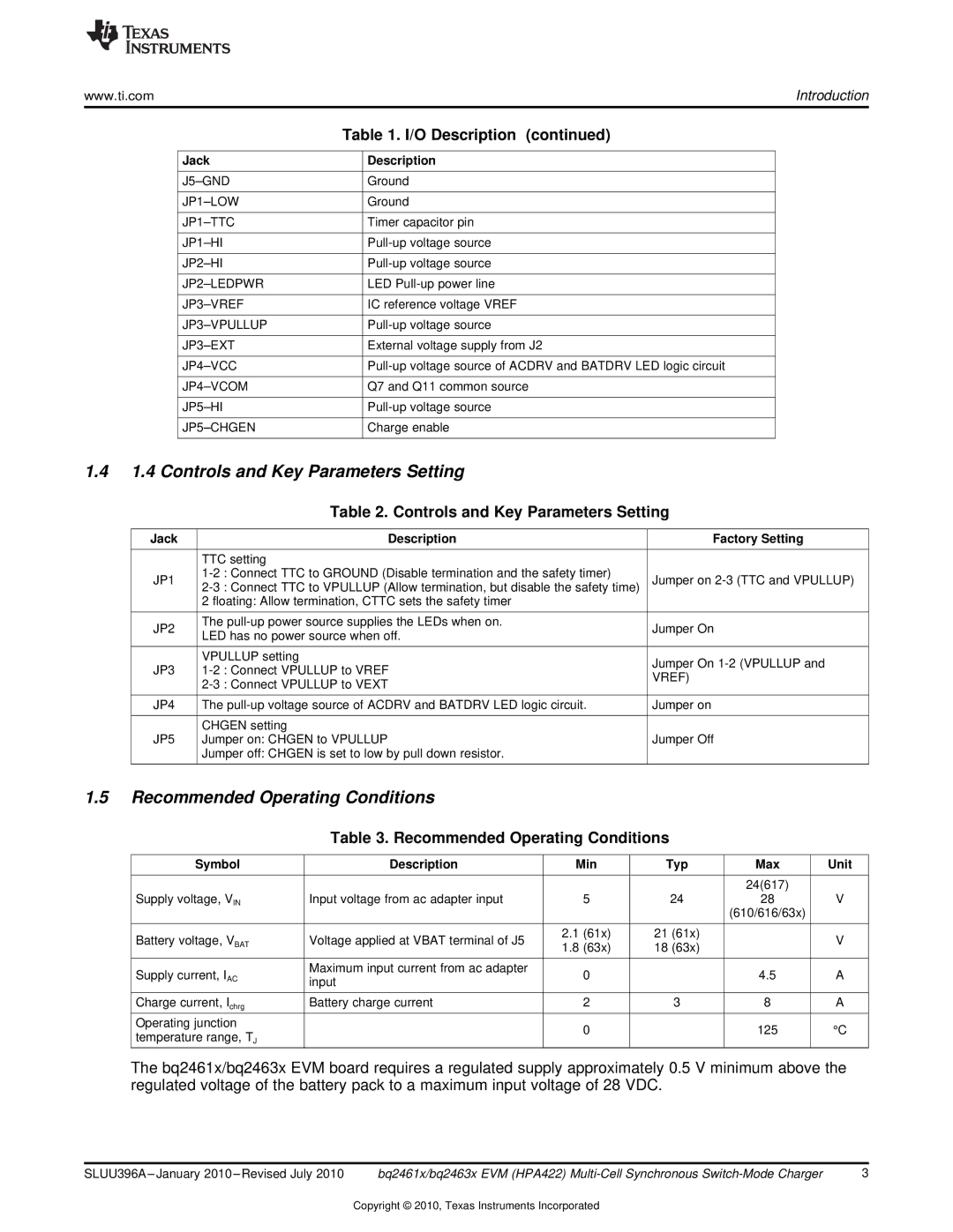
| Table 1. I/O Description (continued) | |
|
|
|
Jack |
| Description |
|
|
|
| Ground | |
|
|
|
| Ground | |
|
|
|
| Timer capacitor pin | |
|
|
|
| ||
|
|
|
| ||
|
|
|
| LED | |
|
|
|
| IC reference voltage VREF | |
|
|
|
| ||
|
|
|
| External voltage supply from J2 | |
|
|
|
| ||
|
|
|
| Q7 and Q11 common source | |
|
|
|
| ||
|
|
|
| Charge enable | |
|
|
|
1.41.4 Controls and Key Parameters Setting
Table 2. Controls and Key Parameters Setting
Jack |
| Description | Factory Setting | |
|
|
| ||
| TTC setting |
| ||
JP1 | : Connect TTC to GROUND (Disable termination and the safety timer) | Jumper on | ||
: Connect TTC to VPULLUP (Allow termination, but disable the safety time) | ||||
|
| |||
| 2 floating: Allow termination, CTTC sets the safety timer |
| ||
|
|
| ||
JP2 | The | Jumper On | ||
LED has no power source when off. | ||||
|
| |||
|
|
| ||
| VPULLUP setting | Jumper On | ||
JP3 | : Connect VPULLUP to VREF | |||
VREF) | ||||
| : Connect VPULLUP to VEXT | |||
|
| |||
|
|
| ||
JP4 | The | Jumper on | ||
|
|
| ||
| CHGEN setting |
| ||
JP5 | Jumper on: CHGEN to VPULLUP | Jumper Off | ||
| Jumper off: CHGEN is set to low by pull down resistor. |
| ||
|
|
|
| |
1.5Recommended Operating Conditions
Table 3. Recommended Operating Conditions
Symbol | Description | Min | Typ | Max | Unit |
|
|
|
|
|
|
|
|
|
| 24(617) |
|
Supply voltage, VIN | Input voltage from ac adapter input | 5 | 24 | 28 | V |
|
|
|
| (610/616/63x) |
|
|
|
|
|
|
|
Battery voltage, VBAT | Voltage applied at VBAT terminal of J5 | 2.1 (61x) | 21 (61x) |
| V |
1.8 (63x) | 18 (63x) |
| |||
|
|
|
| ||
|
|
|
|
|
|
Supply current, IAC | Maximum input current from ac adapter | 0 |
| 4.5 | A |
input |
| ||||
|
|
|
|
| |
|
|
|
|
|
|
Charge current, Ichrg | Battery charge current | 2 | 3 | 8 | A |
|
|
|
|
|
|
Operating junction |
| 0 |
| 125 | °C |
temperature range, TJ |
|
| |||
|
|
|
|
|
The bq2461x/bq2463x EVM board requires a regulated supply approximately 0.5 V minimum above the regulated voltage of the battery pack to a maximum input voltage of 28 VDC.
SLUU396A | bq2461x/bq2463x EVM (HPA422) | 3 |
Copyright © 2010, Texas Instruments Incorporated
