www.ti.com | Analog Interface |
2Analog Interface
For maximum flexibility, the DAC7716EVM can interface to multiple analog sources. Samtec part numbers
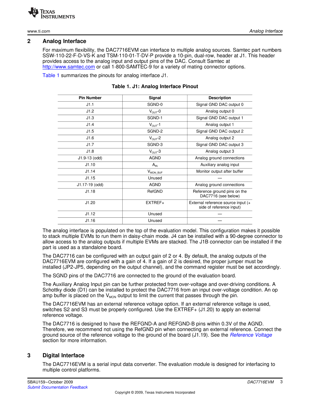
Table 1 summarizes the pinouts for analog interface J1.
Table 1. J1: Analog Interface Pinout
Pin Number | Signal | Description |
|
|
|
J1.1 | Signal GND DAC output 0 | |
|
|
|
J1.2 | Analog output 0 | |
J1.3 | Signal GND DAC output 1 | |
|
|
|
J1.4 | Analog output 1 | |
|
|
|
J1.5 | Signal GND DAC output 2 | |
|
|
|
J1.6 | Analog output 2 | |
J1.7 | Signal GND DAC output 3 | |
|
|
|
J1.8 | Analog output 3 | |
AGND | Analog ground connections | |
|
|
|
J1.10 | AIN | Auxiliary analog input |
J1.14 | VMON_BUF | Monitor output after buffer |
J1.15 | Unused | — |
|
|
|
AGND | Analog ground connections | |
|
|
|
J1.18 | RefGND | Reference ground pins on the |
|
| DAC7716 (see below) |
|
|
|
J1.20 | EXTREF+ | External reference source input (+ |
|
| side of reference input) |
|
|
|
J1.12 | Unused | — |
|
|
|
J1.16 | Unused | — |
|
|
|
The analog interface is populated on the top of the evaluation model. This configuration makes it possible to stack multiple EVMs to run them in
The DAC7716 can be configured with an output gain of 2 or 4. By default, the analog outputs of the DAC7716EVM are configured with a gain of 4. If a gain of 2 is desired, the proper jumper must be installed
The SGND pins of the DAC7716 are connected to the ground of the evaluation board.
The Auxiliary Analog Input pin can be further protected from
The DAC7716EVM has an external reference voltage option. If an external reference voltage is used, switches S2 and S3 must be properly configured. Use the EXTREF+ (J1.20) to apply an external reference voltage.
The DAC7716 is designed to have the
3Digital Interface
The DAC7716EVM is a serial input data converter. The evaluation module is designed for interfacing to multiple control platforms.
SBAU159 | DAC7716EVM 3 |
Submit Documentation Feedback |
|
Copyright © 2009, Texas Instruments Incorporated