Digital Interface | www.ti.com |
3.1Serial Data Interface
Samtec part numbers
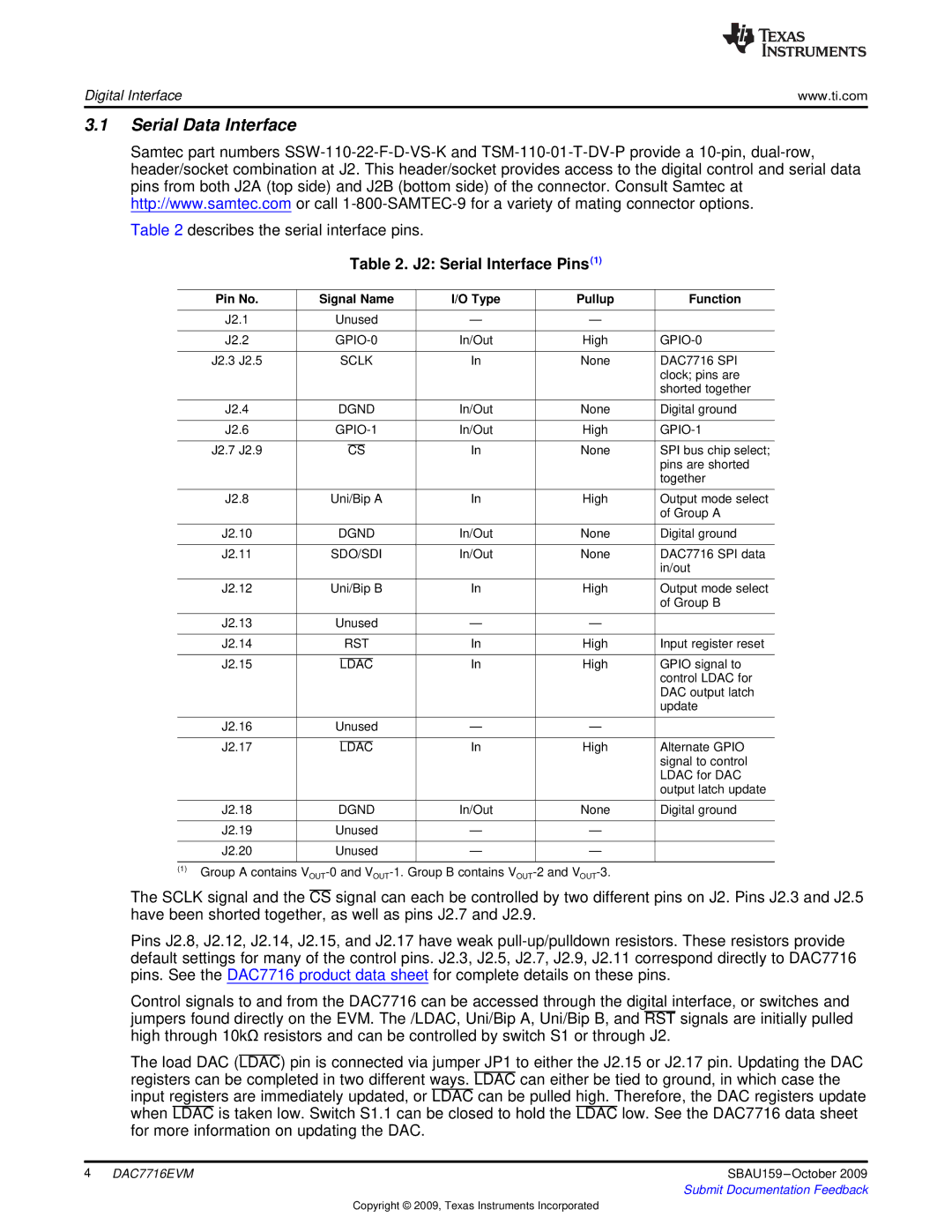
Table 2 describes the serial interface pins.
Table 2. J2: Serial Interface Pins(1)
Pin No. | Signal Name | I/O Type | Pullup | Function | |||||
|
|
|
|
| |||||
J2.1 | Unused | — | — |
| |||||
|
|
|
|
| |||||
J2.2 | In/Out | High | |||||||
|
|
|
|
|
| ||||
J2.3 J2.5 |
| SCLK | In | None | DAC7716 SPI | ||||
|
|
|
|
|
|
|
|
| clock; pins are |
|
|
|
|
|
|
|
|
| shorted together |
|
|
|
|
| |||||
J2.4 | DGND | In/Out | None | Digital ground | |||||
|
|
|
|
| |||||
J2.6 | In/Out | High | |||||||
|
|
|
|
|
|
|
| ||
J2.7 J2.9 |
|
|
|
| In | None | SPI bus chip select; | ||
|
| CS | |||||||
|
|
|
|
|
|
|
|
| pins are shorted |
|
|
|
|
|
|
|
|
| together |
|
|
|
|
|
|
| |||
J2.8 | Uni/Bip A | In | High | Output mode select | |||||
|
|
|
|
|
|
|
|
| of Group A |
|
|
|
|
|
|
| |||
J2.10 | DGND | In/Out | None | Digital ground | |||||
|
|
|
|
|
|
| |||
J2.11 | SDO/SDI | In/Out | None | DAC7716 SPI data | |||||
|
|
|
|
|
|
|
|
| in/out |
|
|
|
|
|
|
| |||
J2.12 | Uni/Bip B | In | High | Output mode select | |||||
|
|
|
|
|
|
|
|
| of Group B |
|
|
|
|
|
|
| |||
J2.13 | Unused | — | — |
| |||||
|
|
|
|
|
|
|
| ||
J2.14 |
| RST | In | High | Input register reset | ||||
|
|
|
|
|
|
|
|
| |
J2.15 |
|
|
|
|
| In | High | GPIO signal to | |
| LDAC | ||||||||
|
|
|
|
|
|
|
|
| control LDAC for |
|
|
|
|
|
|
|
|
| DAC output latch |
|
|
|
|
|
|
|
|
| update |
|
|
|
|
|
|
|
| ||
J2.16 | Unused | — | — |
| |||||
|
|
|
|
|
|
|
|
|
|
J2.17 |
|
|
|
|
|
| In | High | Alternate GPIO |
| LDAC | ||||||||
|
|
|
|
|
|
|
|
| signal to control |
|
|
|
|
|
|
|
|
| LDAC for DAC |
|
|
|
|
|
|
|
|
| output latch update |
|
|
|
|
|
|
|
|
|
|
J2.18 | DGND | In/Out | None | Digital ground | |||||
|
|
|
|
|
|
|
|
|
|
J2.19 | Unused | — | — |
| |||||
|
|
|
|
|
|
|
|
|
|
J2.20 | Unused | — | — |
| |||||
|
|
|
|
|
|
|
|
|
|
(1)Group A contains
The SCLK signal and the CS signal can each be controlled by two different pins on J2. Pins J2.3 and J2.5 have been shorted together, as well as pins J2.7 and J2.9.
Pins J2.8, J2.12, J2.14, J2.15, and J2.17 have weak
Control signals to and from the DAC7716 can be accessed through the digital interface, or switches and jumpers found directly on the EVM. The /LDAC, Uni/Bip A, Uni/Bip B, and RST signals are initially pulled high through 10kΩ resistors and can be controlled by switch S1 or through J2.
The load DAC (LDAC) pin is connected via jumper JP1 to either the J2.15 or J2.17 pin. Updating the DAC registers can be completed in two different ways. LDAC can either be tied to ground, in which case the input registers are immediately updated, or LDAC can be pulled high. Therefore, the DAC registers update when LDAC is taken low. Switch S1.1 can be closed to hold the LDAC low. See the DAC7716 data sheet for more information on updating the DAC.
4 DAC7716EVM | SBAU159 |
| Submit Documentation Feedback |
Copyright © 2009, Texas Instruments Incorporated