www.ti.com | EVM Operation |
6.3Default Jumper Settings and Switch Positions
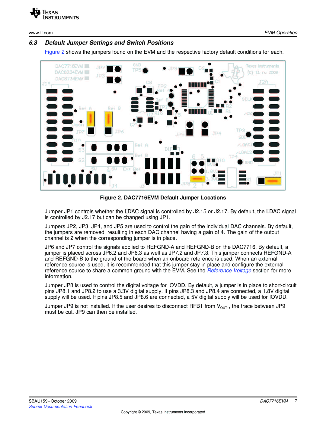
Figure 2 shows the jumpers found on the EVM and the respective factory default conditions for each.
Figure 2. DAC7716EVM Default Jumper Locations
Jumper JP1 controls whether the LDAC signal is controlled by J2.15 or J2.17. By default, the LDAC signal is controlled by J2.17 but can be changed using JP1.
Jumpers JP2, JP3, JP4, and JP5 are used to control the gain of the individual DAC channels. By default, the jumpers are removed, resulting in each DAC channel having a gain of 4. The gain of the output channel is 2 when the corresponding jumper is in place.
JP6 and JP7 control the signals applied to
Jumper JP8 is used to control the digital voltage for IOVDD. By default, a jumper is in place to
Jumper JP9 is not installed. If the user desires to disconnect RFB1 from VOUT1, the trace between JP9 must be cut. JP9 can then be installed.
SBAU159 | DAC7716EVM 7 |
Submit Documentation Feedback |
|
Copyright © 2009, Texas Instruments Incorporated