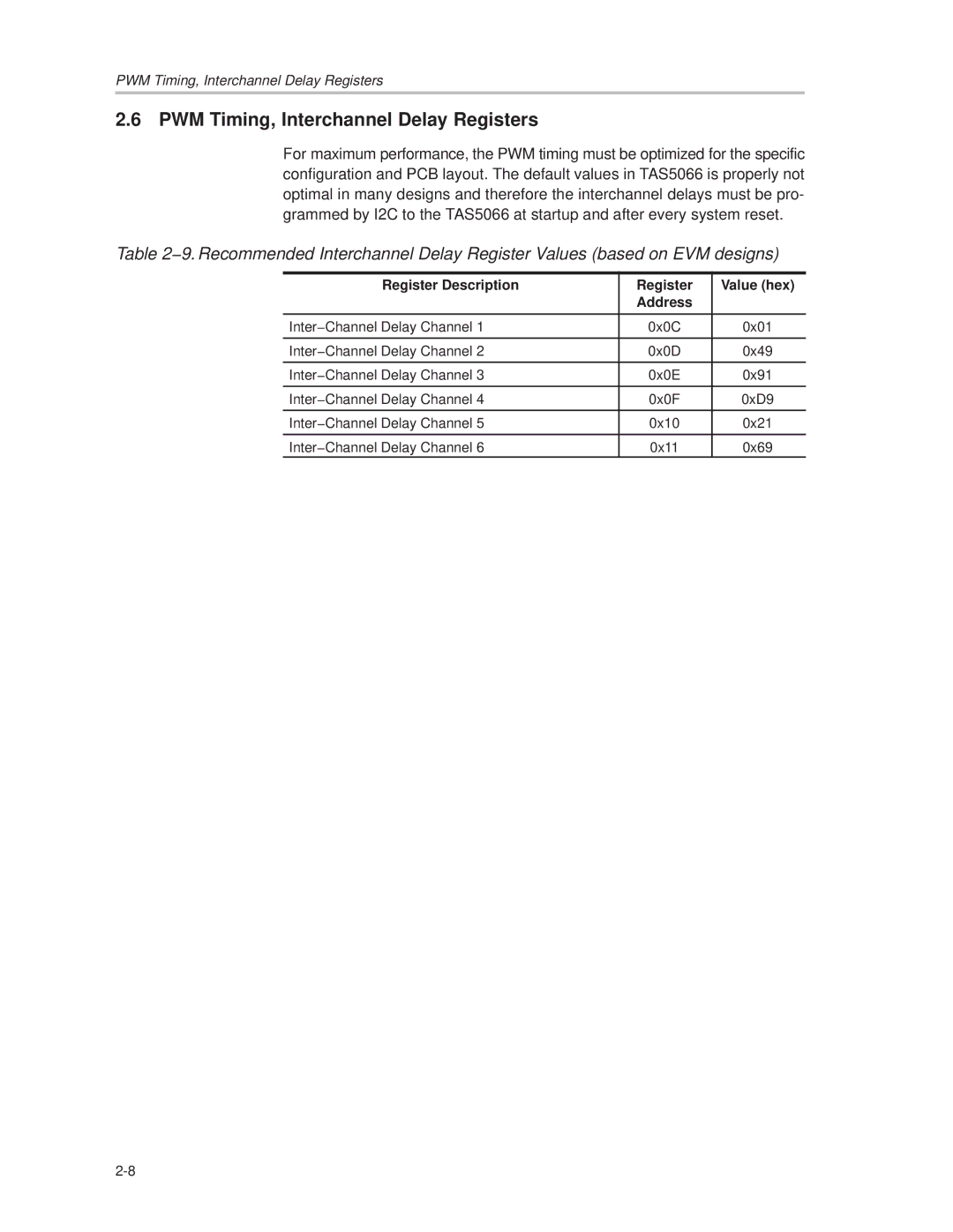
TAS5066PAG specifications
The Texas Instruments TAS5066PAG is a highly efficient Class D audio amplifier designed for high-performance audio applications. Known for its advanced technology and robust features, it is part of a series that is widely used in home audio systems, professional sound equipment, and automotive audio devices.One of the standout features of the TAS5066PAG is its ability to deliver high power output while maintaining low distortion levels. It is capable of providing up to 300W per channel at 4 ohms, making it a powerful solution for driving high-performance loudspeakers. With a total harmonic distortion plus noise (THD+N) rating as low as 0.01%, the device assures clean and clear audio reproduction, which is critical in high-fidelity audio systems.
The TAS5066PAG utilizes a digital input mechanism that supports various audio formats, including I2S and PCM, which allows for versatile integration with various digital audio sources. This feature streamlines the design process for system builders and reduces power consumption by eliminating the need for multiple digital-to-analog converters.
Another significant technological advantage of the TAS5066PAG is its integrated power stage. This integration simplifies circuit design by reducing the number of external components required, subsequently enhancing reliability and reducing the overall size of the audio system. Additionally, the device includes advanced thermal management features that ensure safe and stable operation under varying load conditions, which is especially important for high-power applications.
The TAS5066PAG also offers flexible feedback and control options. Its adaptive feedback loop technology provides real-time adjustments to the audio signal, further improving performance and reducing distortion. This adaptability makes it suitable for a wide range of uses, from consumer electronics to professional systems.
In summary, the Texas Instruments TAS5066PAG is a versatile and powerful Class D amplifier that combines high-performance audio output with advanced digital processing capabilities. Its low distortion, high efficiency, and integrated design elements make it an excellent choice for audio engineers and designers focusing on creating high-quality audio systems. Whether used in home theaters, musical instruments, or automotive audio, the TAS5066PAG sets a high standard for modern audio amplification solutions.