TPS54810 | www.ti.com |
SLVS420B − MARCH 2002 − R EVISED FEBRUARY 2005
APPLICATION INFORMATION
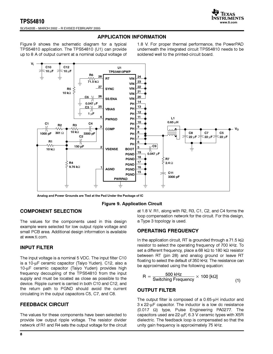
Figure 9 shows the schematic diagram for a typical TPS54810 application. The TPS54810 (U1) can provide up to 8 A of output current at a nominal output voltage of
1.8V. For proper thermal performance, the PowerPAD underneath the integrated circuit TPS54810 needs to be soldered well to the
VI |
|
|
|
|
|
|
|
|
|
|
|
|
|
|
|
|
|
C10 |
| C12 |
|
| U1 |
|
|
|
|
|
|
|
|
|
|
| |
10 ∝F |
| 10 ∝F | R6 |
| TPS54810PWP |
|
|
|
|
|
|
|
|
|
| ||
|
|
|
| 28 | RT | VIN | 24 |
|
|
|
|
|
|
|
|
| |
|
|
|
|
|
|
|
|
|
|
|
|
|
| ||||
|
|
|
| 71.5 kΩ |
| VIN | 23 |
|
|
|
|
|
|
|
|
| |
|
|
| R5 |
| 27 | SYNC | VIN | 22 |
|
|
|
|
|
|
|
|
|
|
| 10 kΩ |
| 26 |
| VIN | 21 |
|
|
|
|
|
|
|
|
| |
|
|
|
| C6 | SS/ENA | VIN | 20 |
|
|
|
|
|
|
|
|
| |
|
|
|
| 0.047 ∝F |
|
| PH | 14 |
|
|
|
|
|
|
|
|
|
|
|
|
| C3 | 25 | VBIAS | PH | 13 |
|
|
|
|
|
|
|
|
|
|
|
|
|
|
| 12 |
|
|
|
|
|
|
|
|
| ||
|
|
|
| 1 ∝F | 4 |
| PH |
|
|
|
|
|
|
|
|
| |
|
|
|
|
| PWRGD | PH | 11 | L1 |
|
|
|
|
|
|
|
| |
C1 | R2 |
| R3 | C4 | 3 |
| PH | 10 | 0.65 ∝H |
|
|
|
|
|
|
|
|
|
|
|
| PH | 9 |
|
|
|
|
|
|
|
| VO | |||
|
|
| 10 kΩ |
| COMP |
|
|
|
|
|
|
|
| ||||
1000 pF | 301 Ω | 3300 pF |
|
| PH | 8 | C8 |
|
| C7 |
|
| C5 |
|
| ||
|
| C2 |
|
| 7 | 22 | ∝ | F | 22 | ∝ | F | 22 | ∝ | F | |||
R1 |
|
|
|
|
|
| PH |
|
|
| |||||||
|
| 150 pF | 2 |
| PH | 6 | C9 |
|
|
|
|
|
|
|
| ||
10 kΩ |
|
| VSENSE | BOOT | 5 |
|
|
|
|
|
|
|
| ||||
|
|
|
|
|
|
|
|
|
|
|
|
| |||||
|
|
|
|
|
|
| PGND | 19 | 0.047 ∝F |
|
|
|
|
|
|
|
|
|
|
|
|
|
|
| PGND | 18 | R7 |
|
|
|
|
|
|
|
|
|
|
| R4 |
|
|
| PGND | 17 | 2.4 Ω |
|
|
|
|
|
|
|
|
|
|
| 9.76 kΩ |
| 1 |
| 16 |
|
|
|
|
|
|
|
|
| |
|
|
|
| AGND | PGND |
|
|
|
|
|
|
|
|
| |||
|
|
|
|
|
|
|
|
|
|
|
|
|
| ||||
|
|
|
|
|
|
| PGND | 15 | C11 |
|
|
|
|
|
|
|
|
|
|
|
|
|
|
|
| 3300 pF |
|
|
|
|
|
|
|
| |
|
|
|
|
|
| PWRPAD |
|
|
|
|
|
|
|
|
| ||
|
|
|
|
|
|
|
|
|
|
|
|
|
|
|
| ||
Analog and Power Grounds are Tied at the Pad Under the Package of IC |
|
|
|
|
|
|
|
|
| ||||||||
Figure 9. Application Circuit
COMPONENT SELECTION
The values for the components used in this design example were selected for low output ripple voltage and small PCB area. Additional design information is available at www.ti.com.
INPUT FILTER
The input voltage is a nominal 5 VDC. The input filter C10 is a
FEEDBACK CIRCUIT
The values for these components have been selected to provide low output ripple voltage. The resistor divider network of R1 and R4 sets the output voltage for the circuit
at 1.8 V. R1, along with R2, R3, C1, C2, and C4 forms the loop compensation network for the circuit. For this design, a Type 3 topology is used.
OPERATING FREQUENCY
In the application circuit, RT is grounded through a 71.5 kΩ resistor to select the operating frequency of 700 kHz. To set a different frequency, place a 68 kΩ to 180 kΩ resistor between RT (pin 28) and analog ground or leave RT floating to select the default of 350 kHz. The resistance can be approximated using the following equation:
500 kHz |
|
|
R + Switching Frequency | 100 [kW] | (1) |
OUTPUT FILTER
The output filter is composed of a
8