www.ti.com | TPS54810 |
SLVS420B − MARCH 2002 − R EVISED FEBRUARY 2005
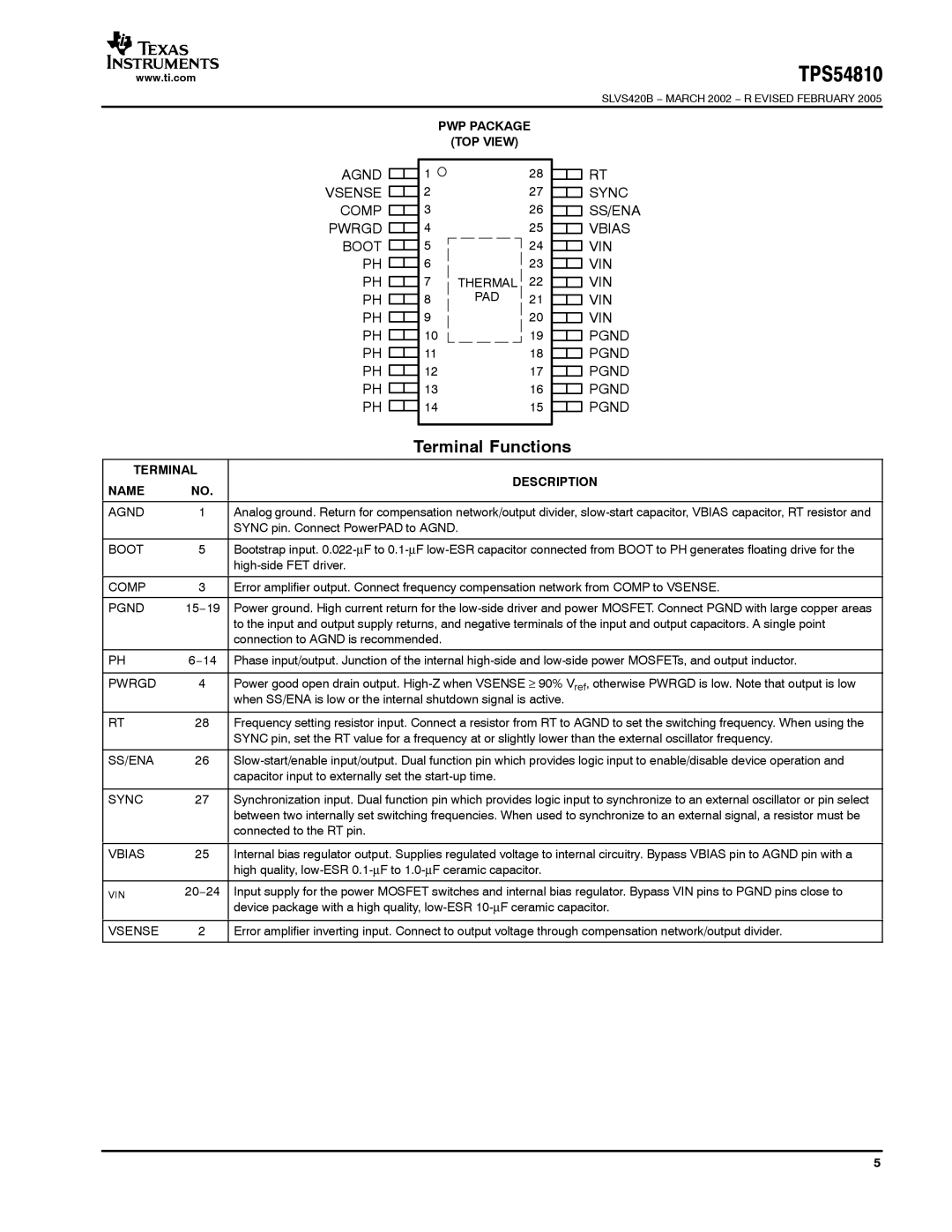
PWP PACKAGE
(TOP VIEW)
AGND ![]()
![]() VSENSE
VSENSE ![]()
![]() COMP
COMP ![]()
![]() PWRGD
PWRGD ![]()
![]() BOOT
BOOT ![]()
![]() PH
PH ![]()
![]() PH
PH ![]()
![]() PH
PH ![]()
![]() PH
PH ![]()
![]() PH
PH ![]()
![]() PH
PH ![]()
![]() PH
PH ![]()
![]() PH
PH ![]()
![]() PH
PH ![]()
![]()
1 | 28 |
227
326
425
524
623
7THERMAL 22
8 | PAD | 21 |
920
1019
1118
1217
1316
1415
RT
![]() SYNC
SYNC
![]() SS/ENA
SS/ENA
![]() VBIAS
VBIAS
![]() VIN
VIN
![]() VIN
VIN
![]() VIN
VIN
![]() VIN
VIN
![]() VIN
VIN
![]() PGND
PGND
![]() PGND
PGND
![]() PGND
PGND
![]() PGND
PGND ![]() PGND
PGND
Terminal Functions
TERMINAL
NAME NO.
DESCRIPTION
AGND | 1 | Analog ground. Return for compensation network/output divider, |
|
| SYNC pin. Connect PowerPAD to AGND. |
|
|
|
BOOT | 5 | Bootstrap input. |
|
| |
|
|
|
COMP | 3 | Error amplifier output. Connect frequency compensation network from COMP to VSENSE. |
|
|
|
PGND | 15−19 | Power ground. High current return for the |
|
| to the input and output supply returns, and negative terminals of the input and output capacitors. A single point |
|
| connection to AGND is recommended. |
|
|
|
PH | 6−14 | Phase input/output. Junction of the internal |
|
|
|
PWRGD | 4 | Power good open drain output. |
|
| when SS/ENA is low or the internal shutdown signal is active. |
|
|
|
RT | 28 | Frequency setting resistor input. Connect a resistor from RT to AGND to set the switching frequency. When using the |
|
| SYNC pin, set the RT value for a frequency at or slightly lower than the external oscillator frequency. |
|
|
|
SS/ENA | 26 | |
|
| capacitor input to externally set the |
|
|
|
SYNC | 27 | Synchronization input. Dual function pin which provides logic input to synchronize to an external oscillator or pin select |
|
| between two internally set switching frequencies. When used to synchronize to an external signal, a resistor must be |
|
| connected to the RT pin. |
|
|
|
VBIAS | 25 | Internal bias regulator output. Supplies regulated voltage to internal circuitry. Bypass VBIAS pin to AGND pin with a |
|
| high quality, |
|
|
|
VIN | 20−24 | Input supply for the power MOSFET switches and internal bias regulator. Bypass VIN pins to PGND pins close to |
|
| device package with a high quality, |
|
|
|
VSENSE 2
Error amplifier inverting input. Connect to output voltage through compensation network/output divider.
5
