www.ti.com
UCC2891EVM Electrical Performance Specifications
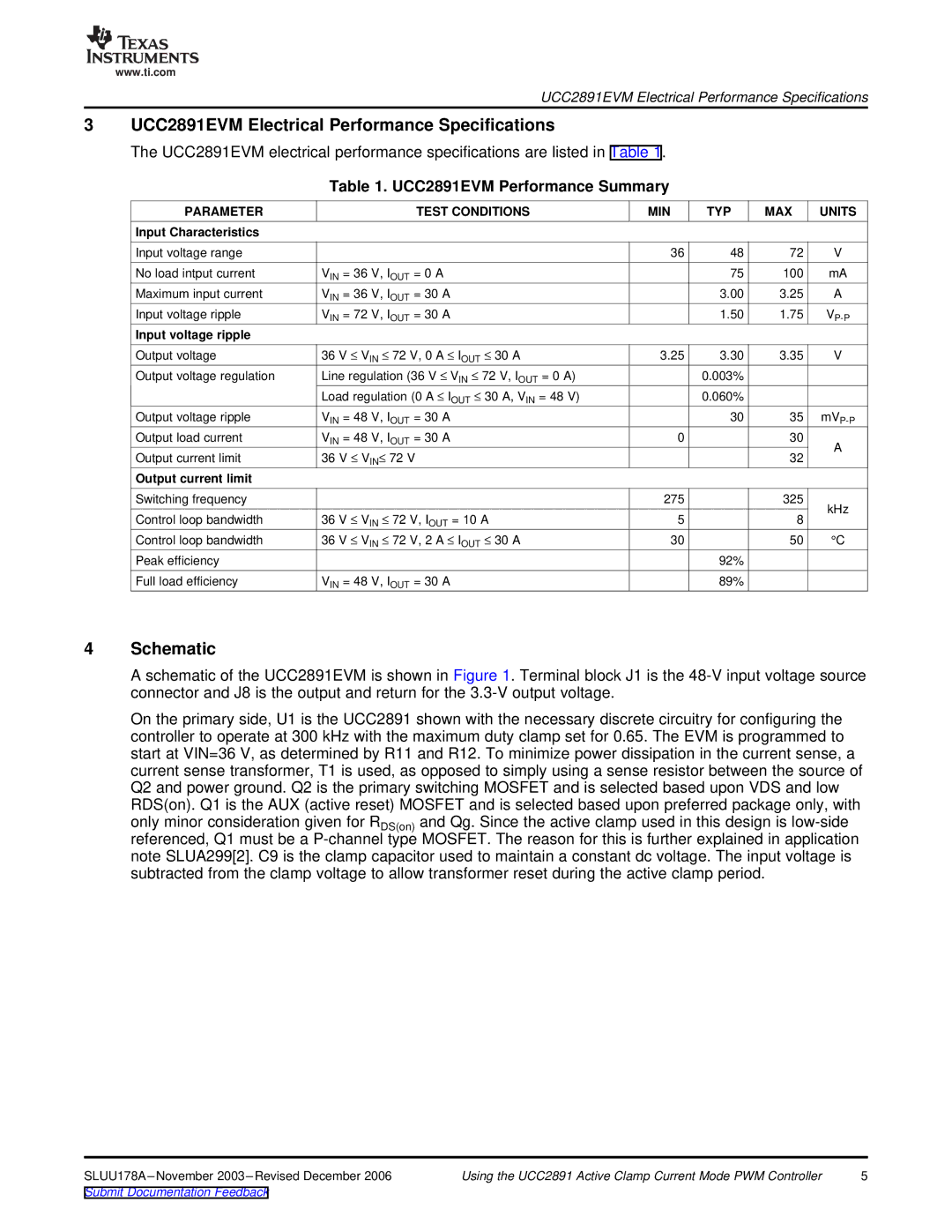
3UCC2891EVM Electrical Performance Specifications
The UCC2891EVM electrical performance specifications are listed in Table 1.
Table 1. UCC2891EVM Performance Summary
PARAMETER | TEST CONDITIONS | MIN | TYP | MAX | UNITS |
Input Characteristics |
|
|
|
|
|
Input voltage range |
| 36 | 48 | 72 | V |
No load intput current | VIN = 36 V, IOUT = 0 A |
| 75 | 100 | mA |
Maximum input current | VIN = 36 V, IOUT = 30 A |
| 3.00 | 3.25 | A |
Input voltage ripple | VIN = 72 V, IOUT = 30 A |
| 1.50 | 1.75 | |
Input voltage ripple |
|
|
|
|
|
Output voltage | 36 V ≤ VIN ≤ 72 V, 0 A ≤ IOUT ≤ 30 A | 3.25 | 3.30 | 3.35 | V |
Output voltage regulation | Line regulation (36 V ≤ VIN ≤ 72 V, IOUT = 0 A) |
| 0.003% |
|
|
| Load regulation (0 A ≤ IOUT ≤ 30 A, VIN = 48 V) |
| 0.060% |
|
|
Output voltage ripple | VIN = 48 V, IOUT = 30 A |
| 30 | 35 | |
Output load current | VIN = 48 V, IOUT = 30 A | 0 |
| 30 | A |
Output current limit | 36 V ≤ VIN≤ 72 V |
|
| 32 | |
|
|
| |||
Output current limit |
|
|
|
|
|
Switching frequency |
| 275 |
| 325 | kHz |
Control loop bandwidth | 36 V ≤ VIN ≤ 72 V, IOUT = 10 A | 5 |
| 8 | |
|
| ||||
Control loop bandwidth | 36 V ≤ VIN ≤ 72 V, 2 A ≤ IOUT ≤ 30 A | 30 |
| 50 | °C |
Peak efficiency |
|
| 92% |
|
|
Full load efficiency | VIN = 48 V, IOUT = 30 A |
| 89% |
|
|
4Schematic
A schematic of the UCC2891EVM is shown in Figure 1. Terminal block J1 is the
On the primary side, U1 is the UCC2891 shown with the necessary discrete circuitry for configuring the controller to operate at 300 kHz with the maximum duty clamp set for 0.65. The EVM is programmed to start at VIN=36 V, as determined by R11 and R12. To minimize power dissipation in the current sense, a current sense transformer, T1 is used, as opposed to simply using a sense resistor between the source of Q2 and power ground. Q2 is the primary switching MOSFET and is selected based upon VDS and low RDS(on). Q1 is the AUX (active reset) MOSFET and is selected based upon preferred package only, with
only minor consideration given for RDS(on) and Qg. Since the active clamp used in this design is
SLUU178A | Using the UCC2891 Active Clamp Current Mode PWM Controller | 5 |
Submit Documentation Feedback