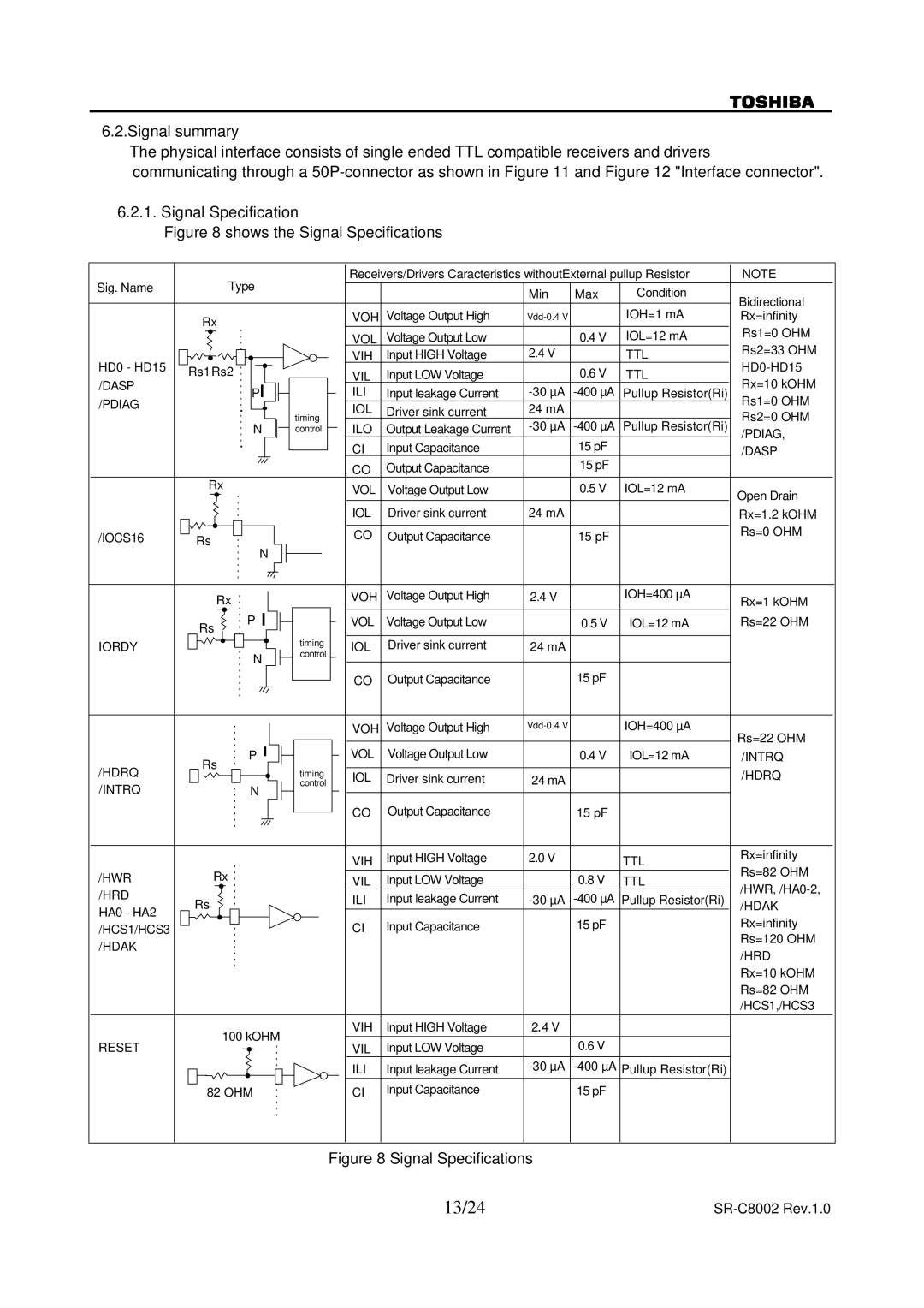
6.2.Signal summary
The physical interface consists of single ended TTL compatible receivers and drivers
communicating through a
6.2.1. Signal Specification
Figure 8 shows the Signal Specifications
Sig. Name | Type |
| Receivers/Drivers Caracteristics withoutExternal pullup Resistor | NOTE | |||||
|
|
| Min | Max | Condition | Bidirectional | |||
|
|
|
|
|
| ||||
|
|
|
|
|
|
|
| IOH=1 mA | |
| Rx |
|
| VOH | Voltage Output High |
| Rx=infinity | ||
|
|
|
|
|
|
| IOL=12 mA | Rs1=0 OHM | |
|
|
|
| VOL | Voltage Output Low |
| 0.4 V | ||
HD0 - HD15 |
|
|
| VIH | Input HIGH Voltage | 2.4 V |
| TTL | Rs2=33 OHM |
Rs1Rs2 |
|
| VIL | Input LOW Voltage |
| 0.6 V | TTL | ||
/DASP |
|
|
| Rx=10 kOHM | |||||
| P |
| ILI | Input leakage Current | Pullup Resistor(Ri) | ||||
/PDIAG |
|
| Rs1=0 OHM | ||||||
|
|
| IOL | Driver sink current | 24 mA |
|
| ||
|
|
| timing |
|
| Rs2=0 OHM | |||
|
| N | ILO | Output Leakage Current | Pullup Resistor(Ri) | ||||
|
| control | /PDIAG, | ||||||
|
|
|
|
| Input Capacitance |
| 15 pF |
| |
|
|
|
| CI |
|
| /DASP | ||
|
|
|
| CO | Output Capacitance |
| 15 pF |
|
|
| Rx |
|
| VOL | Voltage Output Low |
| 0.5 V | IOL=12 mA | Open Drain |
|
|
|
|
|
|
|
|
| |
|
|
|
| IOL | Driver sink current | 24 mA |
|
| Rx=1.2 kOHM |
/IOCS16 | Rs |
|
| CO | Output Capacitance |
| 15 pF |
| Rs=0 OHM |
N |
|
|
|
| |||||
|
|
|
|
|
|
|
|
| |
| Rx |
|
| VOH | Voltage Output High | 2.4 V |
| IOH=400 µA | Rx=1 kOHM |
|
|
|
|
| |||||
| Rs | P |
| VOL | Voltage Output Low |
| 0.5 V | IOL=12 mA | Rs=22 OHM |
|
|
|
|
|
|
|
|
| |
IORDY |
|
| timing | IOL | Driver sink current | 24 mA |
|
|
|
| N | control |
|
|
| ||||
|
|
|
|
|
|
|
| ||
|
|
|
|
|
|
|
|
| |
|
|
|
| CO | Output Capacitance |
| 15 pF |
|
|
|
|
|
| VOH | Voltage Output High |
| IOH=400 µA |
| |
|
|
|
|
|
|
|
|
| Rs=22 OHM |
| Rs | P |
| VOL | Voltage Output Low |
| 0.4 V | IOL=12 mA | /INTRQ |
/HDRQ |
| timing | IOL | Driver sink current |
|
|
| /HDRQ | |
|
| 24 mA |
|
| |||||
/INTRQ |
| N | control |
|
| ||||
|
|
|
|
|
|
|
| ||
|
|
|
| CO | Output Capacitance |
| 15 pF |
|
|
|
|
|
| VIH | Input HIGH Voltage | 2.0 V |
| TTL | Rx=infinity |
/HWR | Rx |
|
| VIL | Input LOW Voltage |
| 0.8 V | TTL | Rs=82 OHM |
|
|
| |||||||
/HRD |
|
|
| ILI | Input leakage Current | Pullup Resistor(Ri) | |||
Rs |
|
| /HDAK | ||||||
HA0 - HA2 |
|
|
|
|
|
|
| ||
|
|
|
| Input Capacitance |
| 15 pF |
| Rx=infinity | |
/HCS1/HCS3 |
|
|
| CI |
|
| |||
/HDAK |
|
|
|
|
|
|
|
| Rs=120 OHM |
|
|
|
|
|
|
|
| /HRD | |
|
|
|
|
|
|
|
|
| |
|
|
|
|
|
|
|
|
| Rx=10 kOHM |
|
|
|
|
|
|
|
|
| Rs=82 OHM |
|
|
|
|
|
|
|
|
| /HCS1,/HCS3 |
| 100 kOHM |
| VIH | Input HIGH Voltage | 2.4 V |
|
|
| |
RESET |
| VIL | Input LOW Voltage |
| 0.6 V |
|
| ||
|
|
|
|
|
| ||||
|
|
|
| ILI | Input leakage Current |
| |||
| 82 OHM |
| CI | Input Capacitance |
| 15 pF |
|
| |
Figure 8 Signal Specifications
13/24 |
|