R
ChipScope PLBv46 IBA (Bus Analyzer) (v1.00a)
assigned for this match group. When multiple match units are available, sequences of a match unit group can be detected. For example, in MU_2, a trigger sequence could be created to look for PLB_PAValid=1 followed by a rising edge on PLB_SaddrAck. For this specific trigger event the first match unit of MU_2 would be set to PLB_PAValid=1 and the second to PLB_SaddrAck=R.
Design Implementation
The ChipScope PLB IBA design is implemented in a Tcl script. When the EDK Platgen tool is run, this Tcl script is called and it internally calls the ChipScope Pro Core generator in command line mode providing a generated argument (.arg) file to create a customized ILA. This ILA is customized per the IBA settings and is attached to the PLB46 bus using a custom HDL wrapper.
Allowable Parameter Combinations
All parameters are independent of each other. Each parameter must be in the range or exact value listed in the allowable values of Table 2. Certain combinations will disable the
Depending on the architecture certain parameters may fail during a design rule check. For instance, if you specify C_NUM_DATA_SAMPLES to be 32768 for a
XST is the synthesis tool used for synthesizing the wrapper HDL generated for the ChipScope PLB IBA. The EDIF netlist output from XST and ChipScope Core Generator are then input to the Xilinx Foundation tool suite for actual device implementation.
Target Technology
The intended target technology is all Xilinx FPGAs.
Device Utilization and Performance Benchmarks
The device utilization varies widely based on the parameter combinations set by the user.
ChipScope PLB46 IBA Module Register Descriptions
Not applicable.
ChipScope PLB46 IBA Module Interrupt Descriptions
Not applicable.
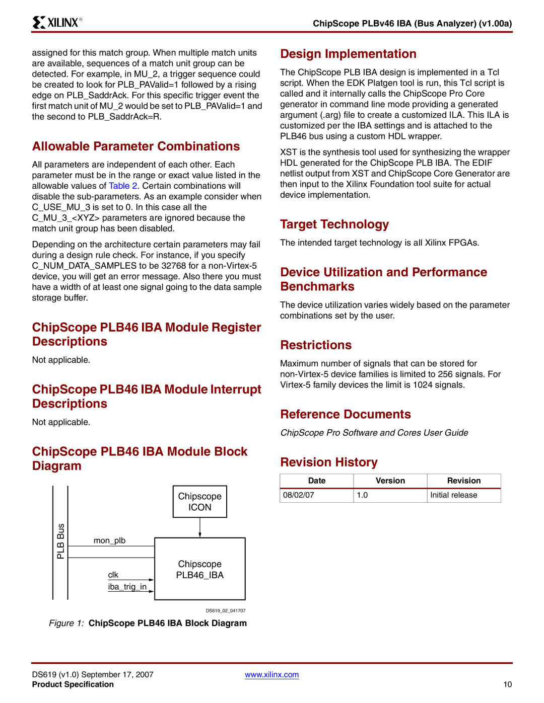
ChipScope PLB46 IBA Module Block Diagram
Restrictions
Maximum number of signals that can be stored for
Reference Documents
ChipScope Pro Software and Cores User Guide
Revision History
PLB Bus
mon_plb
clk
iba_trig_in
Chipscope
ICON
Chipscope
PLB46_IBA
DS619_02_041707
Date |
| Version | Revision |
08/02/07 | 1.0 |
| Initial release |
|
|
|
|
Figure 1: ChipScope PLB46 IBA Block Diagram
DS619 (v1.0) September 17, 2007 | www.xilinx.com |
Product Specification | 10 |