Chapter 3 | |
|
|
3-4. Advanced Chipset Features
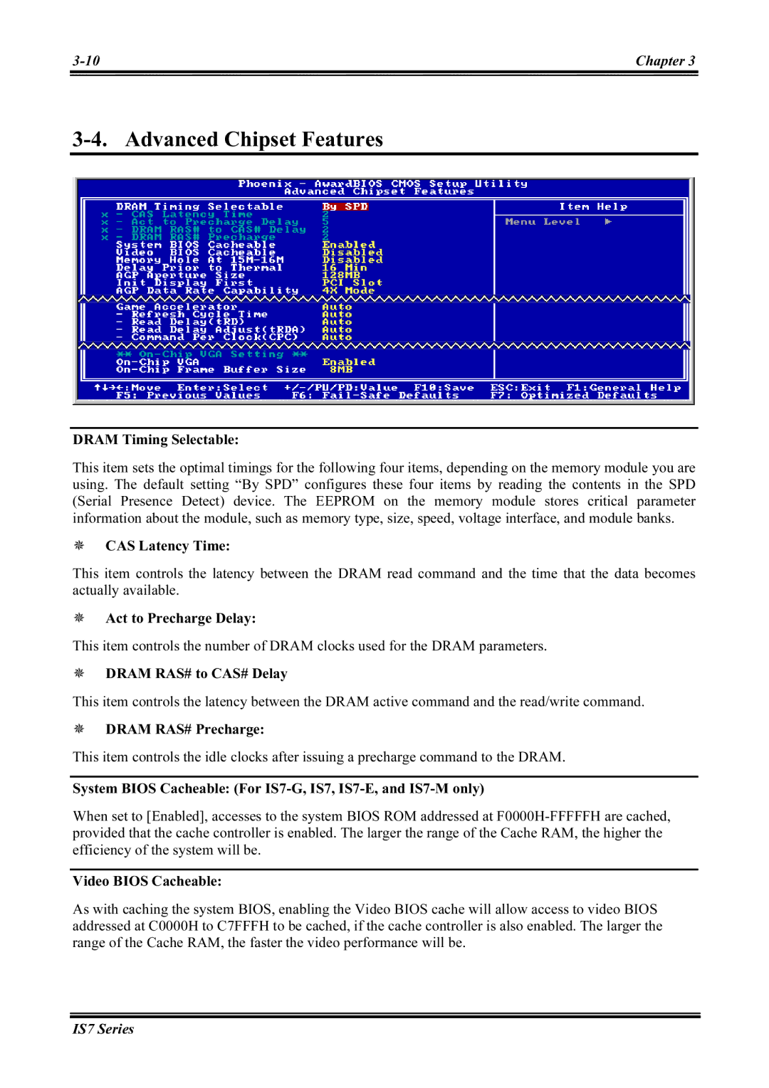
DRAM Timing Selectable:
This item sets the optimal timings for the following four items, depending on the memory module you are using. The default setting “By SPD” configures these four items by reading the contents in the SPD (Serial Presence Detect) device. The EEPROM on the memory module stores critical parameter information about the module, such as memory type, size, speed, voltage interface, and module banks.
CAS Latency Time:
This item controls the latency between the DRAM read command and the time that the data becomes actually available.
Act to Precharge Delay:
This item controls the number of DRAM clocks used for the DRAM parameters.
DRAM RAS# to CAS# Delay
This item controls the latency between the DRAM active command and the read/write command.
DRAM RAS# Precharge:
This item controls the idle clocks after issuing a precharge command to the DRAM.
System BIOS Cacheable: (For
When set to [Enabled], accesses to the system BIOS ROM addressed at
Video BIOS Cacheable:
As with caching the system BIOS, enabling the Video BIOS cache will allow access to video BIOS addressed at C0000H to C7FFFH to be cached, if the cache controller is also enabled. The larger the range of the Cache RAM, the faster the video performance will be.