FEATURES
Broadband RF port: LF to 500 MHz
Conversion gain: 3.7 dB
Noise figure: 12.2 dB
Input IP3: 22.7 dBm
Input P1dB: 8.3 dBm
LO drive: 0 dBm
Differential high impedance RF input port
Exposed paddle LFCSP: 3 mm × 3 mm
APPLICATIONS
Cellular base station receivers
ISM receivers
Radio links
RF instrumentation
GENERAL DESCRIPTION
The AD8342 is a high performance, broadband active mixer. It is well suited for demanding
The AD8342 provides a typical conversion gain of 3.7 dB with an RF frequency of 238 MHz. The integrated LO driver presents a 50 Ω input impedance with a low LO drive level, helping to minimize the external component count.
The differential high impedance broadband RF port allows for easy interfacing to both active devices and passive filters. The RF input accepts input signals as large as 1.6 V
Rev. 0
Information furnished by Analog Devices is believed to be accurate and reliable. However, no responsibility is assumed by Analog Devices for its use, nor for any infringements of patents or other rights of third parties that may result from its use. Specifications subject to change without notice. No license is granted by implication or otherwise under any patent or patent rights of Analog Devices. Trademarks and registered trademarks are the property of their respective owners.
Active Receive Mixer
LF to 500 MHz
AD8342
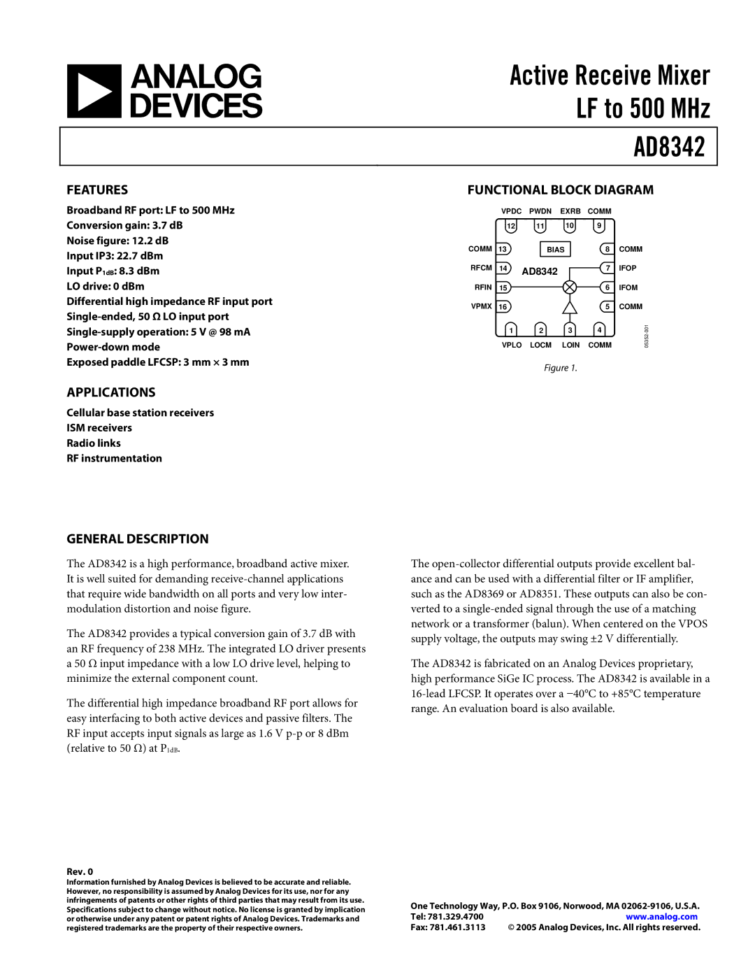
FUNCTIONAL BLOCK DIAGRAM
| VPDC | PWDN | EXRB | COMM |
| |
| 12 | 11 | 10 | 9 |
| |
COMM | 13 |
| BIAS | 8 | COMM | |
RFCM | 14 | AD8342 |
| 7 | IFOP | |
RFIN | 15 |
|
|
| 6 | IFOM |
VPMX | 16 |
|
|
| 5 | COMM |
|
| 1 | 2 | 3 | 4 | |
| VPLO | LOCM | LOIN | COMM | ||
Figure 1.
The
The AD8342 is fabricated on an Analog Devices proprietary, high performance SiGe IC process. The AD8342 is available in a
One Technology Way, P.O. Box 9106, Norwood, MA
Tel: 781.329.4700www.analog.com
Fax: 781.461.3113 © 2005 Analog Devices, Inc. All rights reserved.
