AD8342 | Preliminary Technical Data |
|
|
OUTLINE DIMENSIONS
3.00
![]() BSC SQ
BSC SQ ![]()
PIN 1 | TOP |
INDICATOR | VIEW |
|
|
| 0.50 |
| |
|
|
| 0.40 |
| |
| 0.60 MAX |
| 0.30 | PIN 1 | |
|
|
|
| INDICATOR | |
0.45 | 13 | 16 | 1 | *1.65 | |
1.50 SQ | |||||
| 12 |
| |||
2.75 |
|
|
| 1.35 | |
BSC SQ |
| EXPOSED |
|
| |
|
| PAD |
|
|
0.50 | 9 | (BOTTOM VIEW) 4 | |
| 8 | 5 | |
BSC |
|
| 0.25 MIN |
12° MAX |
| 0.80 MAX | 1.50 REF |
|
| ||
0.90 |
| 0.65 TYP |
|
|
|
| |
0.85 |
| 0.05 MAX |
|
0.80 |
|
| |
| 0.02 NOM |
| |
SEATING | 0.30 |
| |
|
| ||
PLANE | 0.20 REF |
| |
0.23 |
| ||
|
|
| |
| 0.18 |
|
|
*COMPLIANT TO JEDEC STANDARDS
EXCEPT FOR EXPOSED PAD DIMENSION.
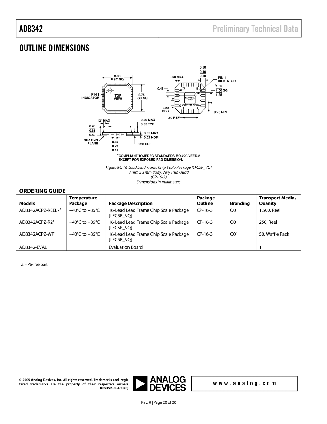
Figure 54. 16-Lead Lead Frame Chip Scale Package [LFCSP_VQ]
3 mm x 3 mm Body, Very Thin Quad
(CP-16-3)
Dimensions in millimeters
ORDERING GUIDE
| Temperature |
| Package |
| Transport Media, |
Models | Package | Package Description | Outline | Branding | Quanity |
|
|
|
|
|
|
−40°C to +85°C | Q01 | 1,500, Reel | |||
|
| [LFCSP_VQ] |
|
|
|
−40°C to +85°C | Q01 | 250, Reel | |||
|
| [LFCSP_VQ] |
|
|
|
−40°C to +85°C | Q01 | 50, Waffle Pack | |||
|
| [LFCSP_VQ] |
|
|
|
|
| Evaluation Board |
|
| 1 |
|
|
|
|
|
|
1Z = Pb-free part.
© 2005 Analog Devices, Inc. All rights reserved. Trademarks and regis- tered trademarks are the property of their respective owners.
Rev. 0 Page 20 of 20
