AD8342
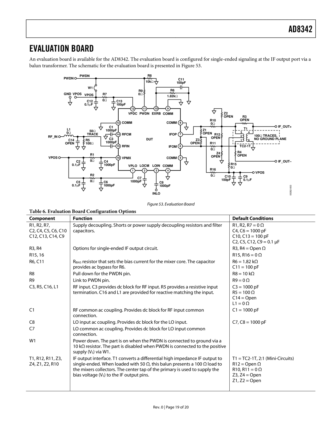
EVALUATION BOARD
An evaluation board is available for the AD8342. The evaluation board is configured for
PWDN | PWDN |
|
| R8 |
|
| C11 |
|
| |
|
|
|
| 10kΩ |
|
|
|
| ||
|
|
|
|
|
| 100pF |
|
| ||
|
| W1 |
|
| R9 |
| R6 |
|
|
|
GND VPOS |
|
|
|
|
|
|
| |||
VPOS | R7 |
| 0Ω |
| Ω |
|
|
| ||
|
|
| 0Ω |
|
|
| 1.82k |
|
|
|
|
| C12 | C13 |
|
|
|
|
|
| |
|
| 0.1∝F |
| 100pF |
|
| 9 |
|
|
|
|
|
|
| 12 | 11 | 10 |
|
|
| |
|
|
|
| VPDC | PWDN EXRB COMM |
| Z2 | R3 | ||
|
|
|
|
|
|
|
|
| OPEN | |
|
|
|
| 13 COMM |
|
| COMM | 8 | R10 | OPEN |
|
|
|
|
|
| 0Ω |
| |||
L1 |
| C1 |
|
|
|
|
| Z1 |
|
| T1 |
| IF_OUT+ | |
50Ω | 1000pF |
|
|
|
|
|
|
|
|
| ||||
|
|
|
|
|
| 3 | 4 |
|
| |||||
0 | Ω | TRACE | 14 | RFCM |
|
| IFOP | 7 | OPEN R12 |
| Ω |
| ||
|
|
|
| 2 | 100 | TRACES, | ||||||||
RF_IN |
| R5 | C3 |
| DUT |
| Z3 | OPEN |
|
| ||||
C14 |
|
| R11 |
| 1 | 6 NO GROUND PLANE | ||||||||
OPEN | 100Ω | 1000pF | RFIN |
|
| IFOM | OPEN |
|
|
| ||||
|
|
| 15 |
|
| 6 | 0Ω |
|
|
| ||||
|
|
|
|
|
|
|
|
|
| R4 |
|
|
| |
|
| R1 |
|
|
|
|
|
| Z4 |
|
|
|
| |
VPOS |
| 16 | VPMX |
|
| COMM | 5 | OPEN |
| OPEN |
|
| ||
C2 | 0Ω |
|
|
|
|
|
|
| IF_OUT– | |||||
| C4 |
|
|
|
|
|
| R15 |
|
|
| |||
| ∝ |
| 1000pF | VPLO | LOCM | LOIN | COMM |
|
|
|
|
|
| |
| 0.1 F |
|
| R16 | 0Ω |
|
|
|
| |||||
|
|
|
| 1 | 2 | 3 | 4 |
|
|
|
|
| ||
|
|
|
|
|
|
| VPOS | |||||||
|
| R2 |
|
|
|
|
|
| 0Ω |
|
| |||
|
|
|
| C7 |
|
|
| C10 |
| C9 |
|
| ||
|
| 0Ω |
|
|
|
|
|
| 100pF |
| 0.1∝F |
|
| |
| C5 | C6 | 1000pF | C8 |
|
|
|
|
| |||||
| 0.1∝F |
| 1000pF |
|
| 1000pF |
|
|
|
|
|
| ||
|
|
|
|
|
| INLO |
|
|
|
|
|
|
| |
| Figure 53. Evaluation Board |
Table 6. Evaluation Board Configuration Options | |
Component | Function |
|
|
R1, R2, R7, | Supply decoupling. Shorts or power supply decoupling resistors and filter |
C2, C4, C5, C6, C10 | capacitors. |
C12, C13, C14, C9 |
|
R3, R4 | Options for |
R15, 16 |
|
R6, C11 | RBIAS resistor that sets the bias current for the mixer core. The capacitor |
| provides ac bypass for R6. |
R8 | Pull down for the PWDN pin. |
R9 | Link to PWDN pin. |
C3, R5, C16, L1 | RF input. C3 provides dc block for RF input. R5 provides a resistive input |
| termination. C16 and L1 are provided for reactive matching the input. |
C1 | RF common ac coupling. Provides dc block for RF input common |
| connection. |
C8 | LO input ac coupling. Provides dc block for the LO input. |
C7 | LO common ac coupling. Provides dc block for LO input common |
| connection. |
W1 | Power down. The part is on when the PWDN is connected to ground via a |
| 10 kΩ resistor. The part is disabled when PWDN is connected to the positive |
| supply (VS) via W1. |
T1, R12, R11, Z3, | IF output interface. T1 converts a differential high impedance IF output to |
Z4, Z1, Z2, R10 | |
| the mixers collectors. The center tap of the primary is used to supply the |
| bias voltage (VS) to the IF output pins. |
|
|
Default Conditions
R1, R2, R7 = 0 Ω C4, C6 = 1000 pF C10, C13 = 100 pF
C2, C5, C12, C9 = 0.1 µF R3, R4 = Open Ω
R15, R16 = 0 Ω
R6 = 1.82 kΩ
C11 = 100 pF
R8 = 10 kΩ
R9 = 0 Ω
C3 = 1000 pF
R5 = 100 Ω
C14 = Open
L1 = 0 Ω
C1 = 1000 pF
C7, C8 = 1000 pF
T1 =
R12 = Open Ω
R10, R11 = 0 Ω
Z3, Z4 = Open
Z1, Z2 = Open
Rev. 0 Page 19 of 20