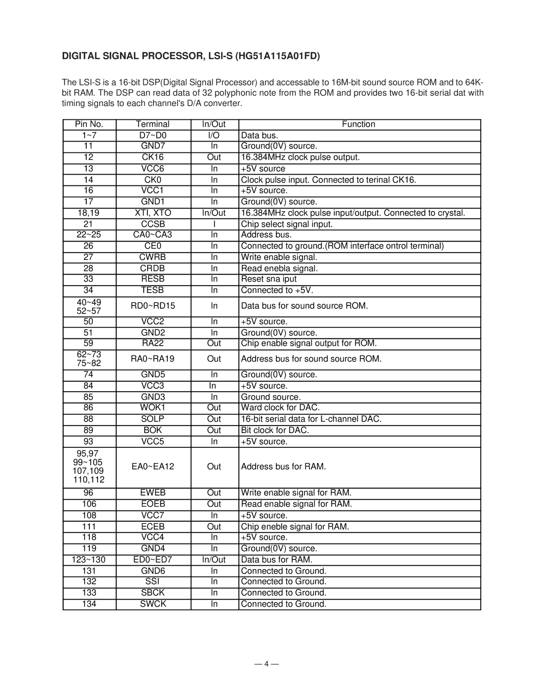
DIGITAL SIGNAL PROCESSOR, LSI-S (HG51A115A01FD)
The
Pin No. | Terminal | In/Out | Function | |
1~7 | D7~D0 | I/O | Data bus. | |
11 | GND7 | In | Ground(0V) source. | |
12 | CK16 | Out | 16.384MHz clock pulse output. | |
13 | VCC6 | In | +5V source | |
14 | CK0 | In | Clock pulse input. Connected to terinal CK16. | |
16 | VCC1 | In | +5V source. | |
17 | GND1 | In | Ground(0V) source. | |
18,19 | XTI, XTO | In/Out | 16.384MHz clock pulse input/output. Connected to crystal. | |
21 | CCSB | I | Chip select signal input. | |
22~25 | CA0~CA3 | In | Address bus. | |
26 | CE0 | In | Connected to ground.(ROM interface ontrol terminal) | |
27 | CWRB | In | Write enable signal. | |
28 | CRDB | In | Read enebla signal. | |
33 | RESB | In | Reset sna iput | |
34 | TESB | In | Connected to +5V. | |
40~49 | RD0~RD15 | In | Data bus for sound source ROM. | |
52~57 | ||||
|
|
| ||
50 | VCC2 | In | +5V source. | |
51 | GND2 | In | Ground(0V) source. | |
59 | RA22 | Out | Chip enable signal output for ROM. | |
62~73 | RA0~RA19 | Out | Address bus for sound source ROM. | |
75~82 | ||||
|
|
| ||
74 | GND5 | In | Ground(0V) source. | |
84 | VCC3 | In | +5V source. | |
85 | GND3 | In | Ground source. | |
86 | WOK1 | Out | Ward clock for DAC. | |
88 | SOLP | Out | ||
89 | BOK | Out | Bit clock for DAC. | |
93 | VCC5 | In | +5V source. | |
95,97 |
|
|
| |
99~105 | EA0~EA12 | Out | Address bus for RAM. | |
107,109 | ||||
|
|
| ||
110,112 |
|
|
| |
|
|
|
| |
96 | EWEB | Out | Write enable signal for RAM. | |
106 | EOEB | Out | Read enable signal for RAM. | |
108 | VCC7 | In | +5V source. | |
111 | ECEB | Out | Chip eneble signal for RAM. | |
118 | VCC4 | In | +5V source. | |
119 | GND4 | In | Ground(0V) source. | |
123~130 | ED0~ED7 | In/Out | Data bus for RAM. | |
131 | GND6 | In | Connected to Ground. | |
132 | SSI | In | Connected to Ground. | |
133 | SBCK | In | Connected to Ground. | |
134 | SWCK | In | Connected to Ground. |
— 4 —