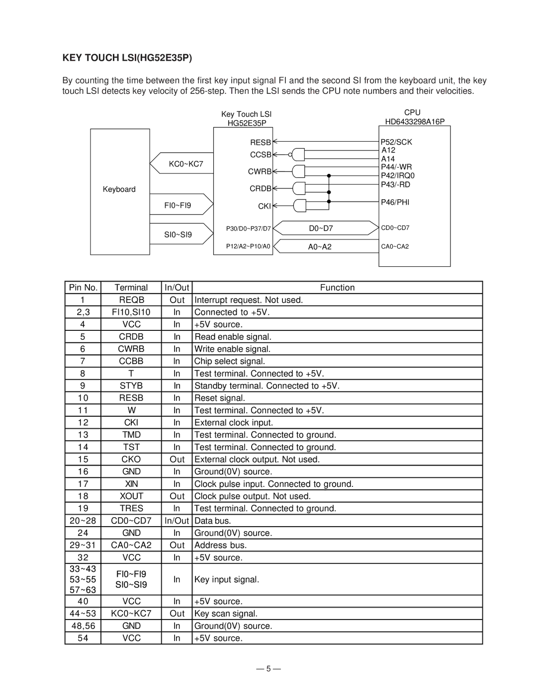
KEY TOUCH LSI(HG52E35P)
By counting the time between the first key input signal FI and the second SI from the keyboard unit, the key touch LSI detects key velocity of
|
|
| Key Touch LSI |
|
|
|
| CPU |
|
|
| HG52E35P |
|
|
|
| HD6433298A16P |
|
|
| RESB |
|
|
|
| P52/SCK |
|
|
| CCSB |
|
|
|
| A12 |
|
|
|
|
|
|
| A14 | |
|
| KC0~KC7 |
|
|
|
| ||
|
|
|
|
|
| |||
|
|
| CWRB |
|
|
|
| |
|
|
|
|
|
|
| P42/IRQ0 | |
|
|
|
|
|
|
|
| |
| Keyboard |
| CRDB |
|
|
|
| |
|
|
|
|
|
| |||
|
|
|
|
|
|
| ||
|
| FI0~FI9 | CKI |
|
|
|
| P46/PHI |
|
|
|
|
|
| |||
|
|
|
|
|
|
| ||
|
| SI0~SI9 | P30/D0~P37/D7 |
| D0~D7 |
| CD0~CD7 | |
|
|
|
|
|
|
|
| |
|
|
| P12/A2~P10/A0 |
| A0~A2 |
| CA0~CA2 | |
|
|
|
|
|
|
|
|
|
Pin No. | Terminal | In/Out |
|
| Function |
|
| |
1 | REQB | Out | Interrupt request. Not used. |
|
|
|
|
|
2,3 | FI10,SI10 | In | Connected to +5V. |
|
|
|
|
|
4 | VCC | In | +5V source. |
|
|
|
|
|
5 | CRDB | In | Read enable signal. |
|
|
|
|
|
6 | CWRB | In | Write enable signal. |
|
|
|
|
|
7 | CCBB | In | Chip select signal. |
|
|
|
|
|
8 | T | In | Test terminal. Connected to +5V. |
|
| |||
9 | STYB | In | Standby terminal. Connected to +5V. |
|
| |||
10 | RESB | In | Reset signal. |
|
|
|
|
|
11 | W | In | Test terminal. Connected to +5V. |
|
| |||
12 | CKI | In | External clock input. |
|
|
|
|
|
13 | TMD | In | Test terminal. Connected to ground. |
|
| |||
14 | TST | In | Test terminal. Connected to ground. |
|
| |||
15 | CKO | Out | External clock output. Not used. |
|
| |||
16 | GND | In | Ground(0V) source. |
|
|
|
|
|
17 | XIN | In | Clock pulse input. Connected to ground. |
|
| |||
18 | XOUT | Out | Clock pulse output. Not used. |
|
| |||
19 | TRES | In | Test terminal. Connected to ground. |
|
| |||
20~28 | CD0~CD7 | In/Out | Data bus. |
|
|
|
|
|
24 | GND | In | Ground(0V) source. |
|
|
|
|
|
29~31 | CA0~CA2 | Out | Address bus. |
|
|
|
|
|
32 | VCC | In | +5V source. |
|
|
|
|
|
33~43 | FI0~FI9 |
|
|
|
|
|
|
|
53~55 | In | Key input signal. |
|
|
|
|
| |
SI0~SI9 |
|
|
|
|
| |||
57~63 |
|
|
|
|
|
|
| |
|
|
|
|
|
|
|
| |
40 | VCC | In | +5V source. |
|
|
|
|
|
44~53 | KC0~KC7 | Out | Key scan signal. |
|
|
|
|
|
48,56 | GND | In | Ground(0V) source. |
|
|
|
|
|
54 | VCC | In | +5V source. |
|
|
|
|
|
— 5 —