POWER AMPLIFIER(LA4598)
LA4598 is
Pin No. | Terminal | In/Out | Function |
1 | Power GND | In | Ground(0V) source. |
2 | Ch1 B.S. | - | Terminal for bootstrap capacitor. |
3 | Ch1 OUT | Out | Channel 1 output. |
4 | VCC | In | +9V source. |
5 | Ch1 N.F. | In | Negative feedback input. |
6 | Ch1 IN | In | Channel 1 input. |
7 | D.C. | - | Terminal for decoupling capacitor. |
8 | Pre GND | In | Ground(0V) source. |
9 | Standby | In | Control signal input. 0V:OFF / +9V:ON |
10 | Ch2 IN | In | Channel 2 input. |
11 | Ch2 N.F. | In | Negative feedback input. |
12 | Ch2 OUT | Out | Channel 2 output. |
13 | Ch2 B.S. | - | Terminal for bootstrap capacitor. |
14 | NC | - | Not used. |
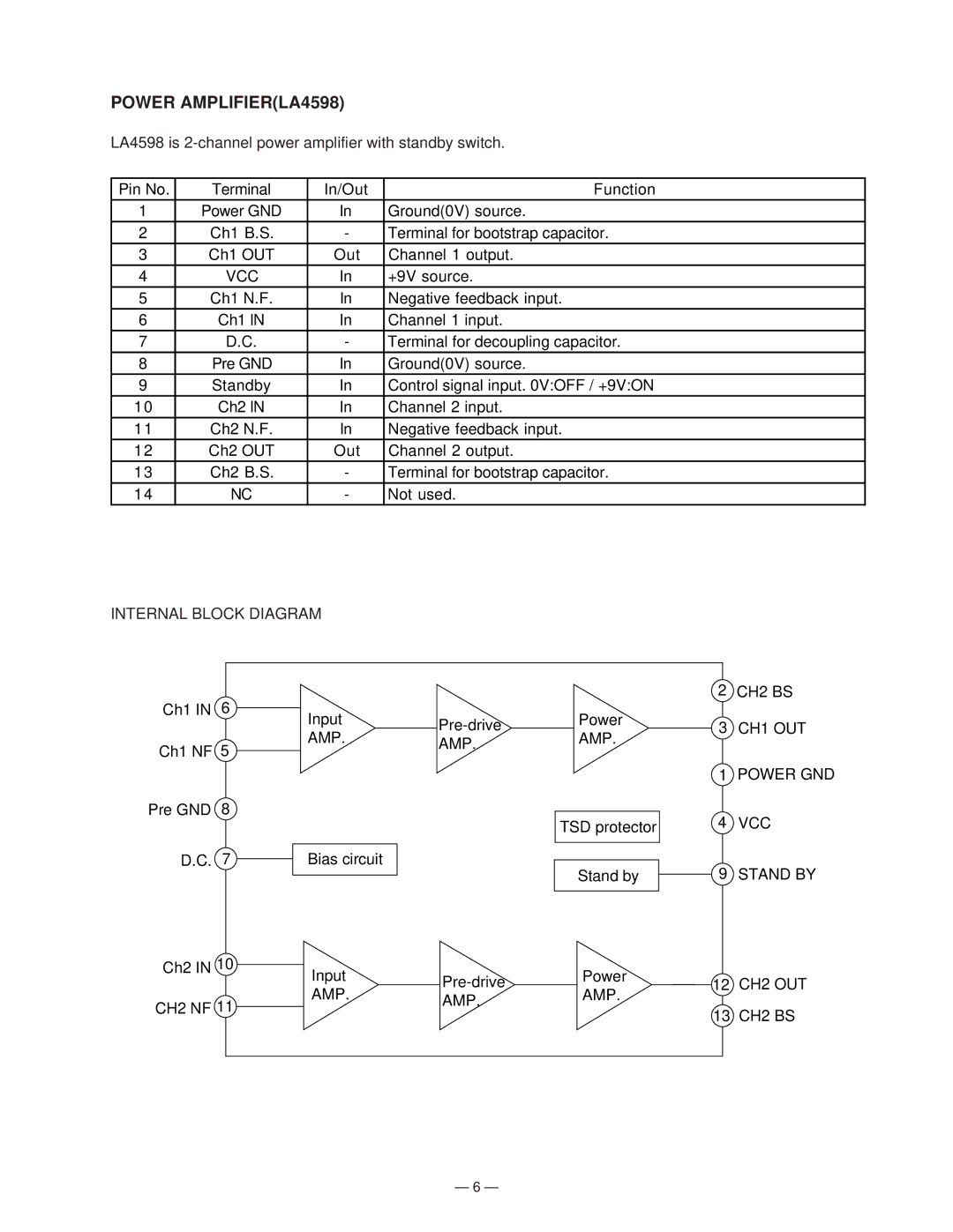
INTERNAL BLOCK DIAGRAM
Ch1 IN 6
Ch1 NF 5
Pre GND 8
Input AMP.
AMP.AMP.
TSD protector
2CH2 BS
3CH1 OUT
1POWER GND
4VCC
D.C. 7 ![]() Bias circuit
Bias circuit
Ch2 IN 10Input
AMP.
CH2 NF 11
Stand by |
| 9 STAND BY |
| ||
|
|
|
Power | 12 | CH2 OUT | ||
AMP. | ||||
AMP. |
|
| ||
|
|
|
13 CH2 BS
— 6 —