CY14E256L
Maximum Ratings
Exceeding maximum ratings may shorten the useful life of the device. These user guidelines are not tested.
Storage Temperature | |
Ambient Temperature with |
|
Power Applied | |
Supply Voltage on VCC Relative to GND | |
Voltage Applied to Outputs | |
in High Z State | |
Input Voltage | |
Transient Voltage (<20 ns) on |
|
Any Pin to Ground Potential |
Package Power Dissipation |
|
Capability (TA = 25°C) | 1.0W |
Surface Mount Lead Soldering |
|
Temperature (3 Seconds) | +260°C |
DC output Current (1 output at a time, 1s duration) .... 15 mA
Static Discharge Voltage | > 2001V |
| |
Latch Up Current | > 200 mA |
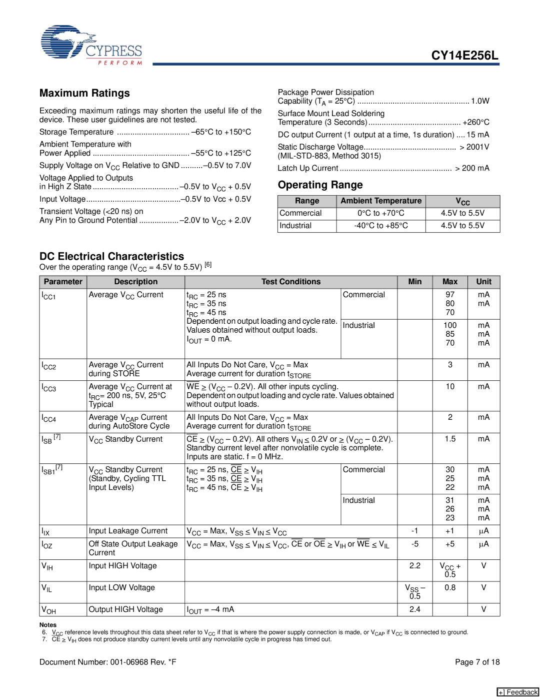
Operating Range
Range | Ambient Temperature | VCC |
Commercial | 0°C to +70°C | 4.5V to 5.5V |
|
|
|
Industrial | 4.5V to 5.5V | |
|
|
|
DC Electrical Characteristics
Over the operating range (VCC = 4.5V to 5.5V) [6]
Parameter | Description |
|
|
|
|
| Test Conditions |
|
|
| Min | Max | Unit | ||||
ICC1 | Average VCC Current | tRC = 25 ns | Commercial |
| 97 | mA | |||||||||||
|
|
| tRC = 35 ns |
|
|
|
| 80 | mA | ||||||||
|
|
| tRC = 45 ns |
|
|
|
| 70 |
| ||||||||
|
|
| Dependent on output loading and cycle rate. |
|
|
|
| ||||||||||
|
|
| Industrial |
| 100 | mA | |||||||||||
|
|
| Values obtained without output loads. |
|
|
|
| 85 | mA | ||||||||
|
|
| IOUT = 0 mA. |
|
|
|
| ||||||||||
|
|
|
|
|
|
| 70 | mA | |||||||||
|
|
|
|
|
|
|
|
|
| ||||||||
ICC2 | Average VCC Current |
| All Inputs Do Not Care, VCC = Max |
|
|
|
| 3 | mA | ||||||||
| during STORE |
| Average current for duration tSTORE |
|
|
|
|
|
| ||||||||
ICC3 | Average VCC Current at |
|
|
| > (VCC – 0.2V). All other inputs cycling. |
|
|
|
| 10 | mA | ||||||
| WE |
|
|
|
| ||||||||||||
| tRC= 200 ns, 5V, 25°C |
| Dependent on output loading and cycle rate. Values obtained |
|
|
| |||||||||||
| Typical |
| without output loads. |
|
|
|
|
|
| ||||||||
ICC4 | Average VCAP Current |
| All Inputs Do Not Care, VCC = Max |
|
|
|
| 2 | mA | ||||||||
| during AutoStore Cycle |
| Average current for duration tSTORE |
|
|
|
|
|
| ||||||||
ISB [7] | VCC Standby Current |
|
| > (VCC – 0.2V). All others VIN < 0.2V or > (VCC – 0.2V). |
| 1.5 | mA | ||||||||||
CE |
| ||||||||||||||||
|
|
| Standby current level after nonvolatile cycle is complete. |
|
|
| |||||||||||
|
|
| Inputs are static. f = 0 MHz. |
|
|
|
|
|
| ||||||||
ISB1[7] | VCC Standby Current |
| tRC = 25 ns, |
| > VIH | Commercial |
| 30 | mA | ||||||||
| CE |
| |||||||||||||||
| (Standby, Cycling TTL |
| tRC = 35 ns, CE > VIH |
|
|
|
| 25 | mA | ||||||||
| Input Levels) |
| tRC = 45 ns, CE > VIH |
|
|
|
| 22 | mA | ||||||||
|
|
|
|
|
|
|
|
|
|
|
| Industrial |
| 31 | mA | ||
|
|
|
|
|
|
|
|
|
|
|
|
|
|
|
| 26 | mA |
|
|
|
|
|
|
|
|
|
|
|
|
|
|
|
| 23 | mA |
IIX | Input Leakage Current | VCC = Max, VSS < VIN < VCC |
|
|
| +1 | μA | ||||||||||
IOZ | Off State Output Leakage |
| VCC = Max, VSS < VIN < VCC, |
| or |
| > VIH or |
| < VIL | +5 | μA | ||||||
| CE | OE | WE | ||||||||||||||
| Current |
|
|
|
|
|
|
|
|
|
|
|
|
|
|
|
|
VIH | Input HIGH Voltage |
|
|
|
|
|
|
|
|
|
|
|
|
| 2.2 | VCC + | V |
|
|
|
|
|
|
|
|
|
|
|
|
|
|
|
| 0.5 |
|
VIL | Input LOW Voltage |
|
|
|
|
|
|
|
|
|
|
|
|
| VSS – | 0.8 | V |
|
|
|
|
|
|
|
|
|
|
|
|
|
|
| 0.5 |
|
|
VOH | Output HIGH Voltage | IOUT = |
|
|
| 2.4 |
| V | |||||||||
Notes
6.VCC reference levels throughout this data sheet refer to VCC if that is where the power supply connection is made, or VCAP if VCC is connected to ground.
7.CE > VIH does not produce standby current levels until any nonvolatile cycle in progress has timed out.
Document Number: | Page 7 of 18 |
[+] Feedback