|
|
|
|
|
|
|
|
|
| CY14E256L | ||
SRAM Write Cycle |
|
|
|
|
|
|
|
|
|
|
| |
Parameter |
| Description |
|
| 25 ns | 35 ns | 45 ns | Unit | ||||
Cypress | Alt |
|
|
| Min | Max | Min | Max | Min | Max | ||
Parameter |
|
|
|
|
| |||||||
|
|
|
|
|
|
|
|
|
|
|
| |
tWC | tAVAV |
| Write Cycle Time |
| 25 |
| 35 |
| 45 |
| ns | |
tPWE | tWLWH, tWLEH |
| Write Pulse Width |
| 20 |
| 25 |
| 30 |
| ns | |
tSCE | tELWH, tELEH |
| Chip Enable To End of Write |
| 20 |
| 25 |
| 30 |
| ns | |
tSD | tDVWH, tDVEH |
| Data Setup to End of Write |
| 10 |
| 12 |
| 15 |
| ns | |
tHD | tWHDX, tEHDX |
| Data Hold After End of Write |
| 0 |
| 0 |
| 0 |
| ns | |
tAW | tAVWH, tAVEH |
| Address Setup to End of Write |
| 20 |
| 25 |
| 30 |
| ns | |
tSA | tAVWL, tAVEL |
| Address Setup to Start of Write |
| 0 |
| 0 |
| 0 |
| ns | |
tHA | tWHAX, tEHAX |
| Address Hold After End of Write |
| 0 |
| 0 |
| 0 |
| ns | |
tHZWE [11,12] | tWLQZ |
| Write Enable to Output Disable |
|
|
| 10 |
| 13 |
| 15 | ns |
tLZWE [11] | tWHQX |
| Output Active After End of Write |
| 5 |
| 5 |
| 5 |
| ns | |
Switching | Waveforms |
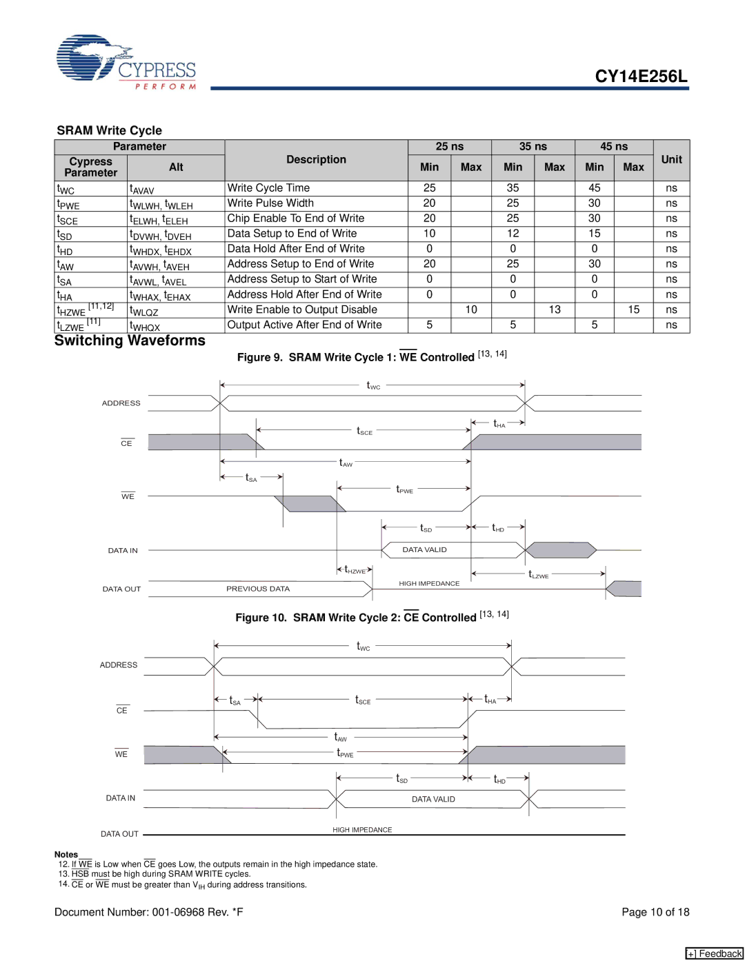
| Figure 9. SRAM Write Cycle 1: |
|
| Controlled [13, 14] |
|
|
|
| ||
|
|
| WE |
|
|
|
| |||||
| tWC |
ADDRESS |
|
| tSCE |
CE |
|
| tAW |
| tSA |
WE | tPWE |
| |
| tSD |
DATA IN | DATA VALID |
| tHZWE |
| HIGH IMPEDANCE |
DATA OUT | PREVIOUS DATA |
tHA
tHD
tLZWE
Figure 10. SRAM Write Cycle 2: CE Controlled [13, 14]
ADDRESS
CE
WE
DATA IN
DATA OUT
tWC
tSA |
|
|
| tSCE |
|
|
| tHA |
|
|
|
| |||||
|
|
|
|
|
|
|
|
|
tAW
tPWE
tSD ![]()
![]() tHD
tHD![]()
DATA VALID
HIGH IMPEDANCE
Notes
12.If WE is Low when CE goes Low, the outputs remain in the high impedance state.
13.HSB must be high during SRAM WRITE cycles.
14.CE or WE must be greater than VIH during address transitions.
Document Number: | Page 10 of 18 |
[+] Feedback