CY14E256L
DC Electrical Characteristics
Over the operating range (continued)(VCC = 4.5V to 5.5V) [6]
Parameter | Description | Test Conditions | Min | Max | Unit | ||
VOL | Output LOW Voltage | IOUT = 8 mA |
| 0.4 | V | ||
VBL | Logic ‘0’ Voltage on |
|
| IOUT = 3 mA |
| 0.4 | V |
HSB |
| ||||||
| Output |
|
|
|
| ||
VCAP | Storage Capacitor | Between VCAP pin and Vss, 6V rated. 68 µF +20% nom. | 54 | 260 | uF | ||
Data Retention and Endurance
Parameter | Description | Min | Unit |
DATAR | Data Retention | 100 | Years |
NVC | Nonvolatile STORE Operations | 1,000 | K |
Capacitance
In the following table, the capacitance parameters are listed.[8]
Parameter |
| Description |
| Test Conditions |
| Max |
|
| Unit |
| |
CIN | Input Capacitance | TA = 25°C, f = 1 MHz, |
| 5 |
|
|
| pF |
| ||
|
|
| VCC = 0 to 3.0V |
|
|
|
|
|
|
| |
COUT | Output Capacitance |
| 7 |
|
|
| pF |
| |||
Thermal Resistance |
|
|
|
|
|
|
|
|
| ||
In the following table, the thermal resistance parameters are listed.[8] |
|
|
|
|
|
|
| ||||
Parameter |
| Description |
| Test Conditions |
|
|
| Unit |
| ||
ΘJA |
| Thermal Resistance |
| Test conditions follow standard test methods | 35.45 |
| TBD | °C/W |
| ||
|
| (Junction to Ambient) |
| and procedures for measuring thermal |
|
|
|
|
|
|
|
|
|
|
| impedance, per EIA / JESD51. |
|
|
|
|
| ||
ΘJC |
| Thermal Resistance |
| 13.26 |
| TBD | °C/W |
| |||
|
| (Junction to Case) |
|
|
|
|
|
|
|
|
|
R1 963Ω
5.0V |
Output |
30 pF
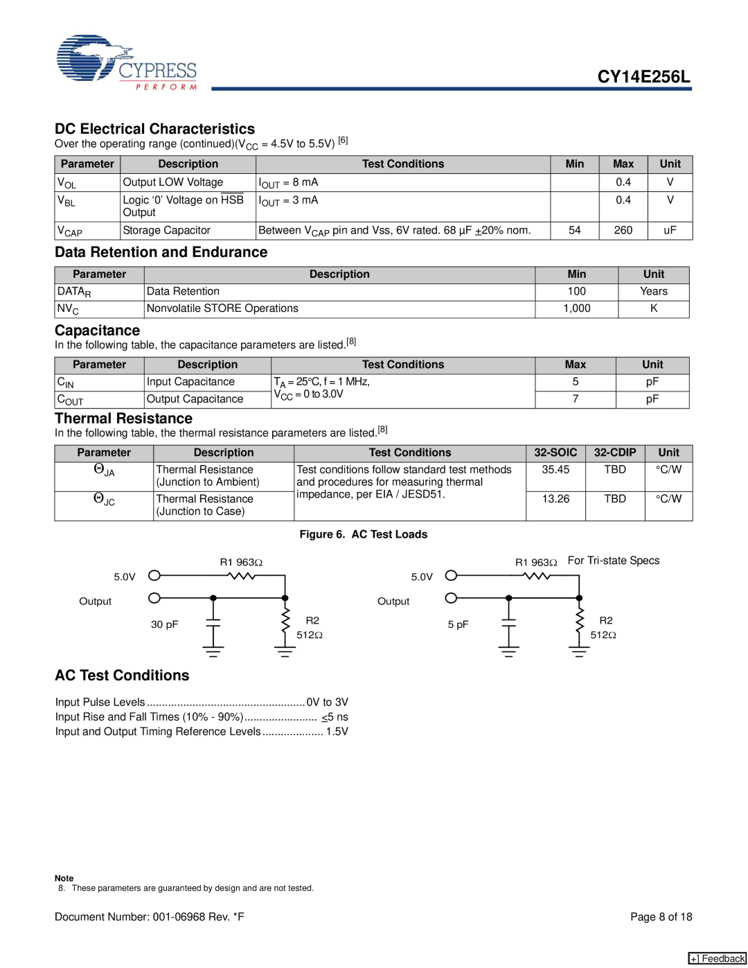
Figure 6. AC Test Loads
R1 963Ω For
5.0V |
Output |
R2 | 5 pF |
|
|
|
|
|
|
|
|
|
|
|
| R2 | |
|
|
|
| ||||||||||||
512Ω |
|
|
|
|
|
|
|
|
|
|
|
| 512Ω | ||
|
|
|
|
|
|
|
|
|
|
|
|
|
| ||
|
|
|
|
|
|
|
|
|
|
|
|
|
| ||
|
|
|
|
|
|
|
|
|
|
|
|
|
|
|
|
|
|
|
|
|
|
|
|
|
|
|
|
|
|
|
|
|
|
|
|
|
|
|
|
|
|
|
|
|
|
|
|
AC Test Conditions
Input Pulse Levels | 0V to 3V |
Input Rise and Fall Times (10% - 90%) | <5 ns |
Input and Output Timing Reference Levels | 1.5V |
Note
8. These parameters are guaranteed by design and are not tested.
Document Number: | Page 8 of 18 |
[+] Feedback