
CY62137FV30 specifications
The Cypress CY62137FV30 is a high-performance SRAM (Static Random Access Memory) device designed for high-speed applications. It features a 4-Mbit memory capacity organized into a 512K x 8-bit configuration, making it suitable for a wide range of embedded systems, computing, and communication applications.One of the standout features of the CY62137FV30 is its fast access time, with speeds as low as 30 ns. This rapid response capability is essential for applications requiring fast data retrieval, such as telecommunications equipment, automotive systems, and consumer electronics where performance is critical. The device also supports a wide operating voltage range from 2.7V to 3.6V, providing flexibility for use in various power-sensitive applications.
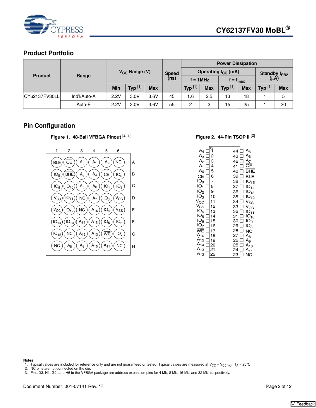
In terms of packaging, the CY62137FV30 is available in compact form factors, allowing for designs with space constraints. It comes in standard packages such as TSOPII and SOJ, which are well-regarded in the industry for ease of integration into circuit boards.
The CY62137FV30 employs advanced CMOS technology, ensuring low power consumption while maintaining high-speed performance. This is particularly beneficial in battery-operated devices where power efficiency is a priority. The device offers both read and write cycles, allowing for seamless data operations. Additionally, the SRAM architecture supports asynchronous operations, allowing users to access memory without the need for a clock signal.
The memory is designed with built-in write protection features, enhancing data integrity during critical operations. It is compatible with various standard memory interfaces, making it easy to integrate into different system architectures. Moreover, the device can endure a significant number of read and write cycles, ensuring durability and reliability over extended use.
The CY62137FV30 also features a simple interface, with easy-to-use control signals, which facilitate straightforward integration and design flexibility. Its ability to handle dynamic data and provide quick access to stored information makes it an excellent choice for applications like networking equipment, industrial automation, and high-performance computing systems.
In summary, the Cypress CY62137FV30 is a versatile SRAM solution that combines high speed, low power consumption, and compact packaging. Its innovative technology and reliable performance make it an excellent choice for various applications requiring efficient and fast memory solutions.