CY62138EV30
MoBL®
2-Mbit (256K x 8) MoBL→ Static RAM
Features
•Very high speed: 45 ns
—Wide voltage range: 2.20V – 3.60V
•
•
—Typical standby current: 1 ∝A
—Maximum standby current: 7 ∝A
•
—Typical active current: 2 mA @ f = 1 MHz
•Easy memory expansion with CE and OE features
•Automatic
•CMOS for optimum speed/power
•Offered in
Functional Description[1]
The CY62138EV30 is a
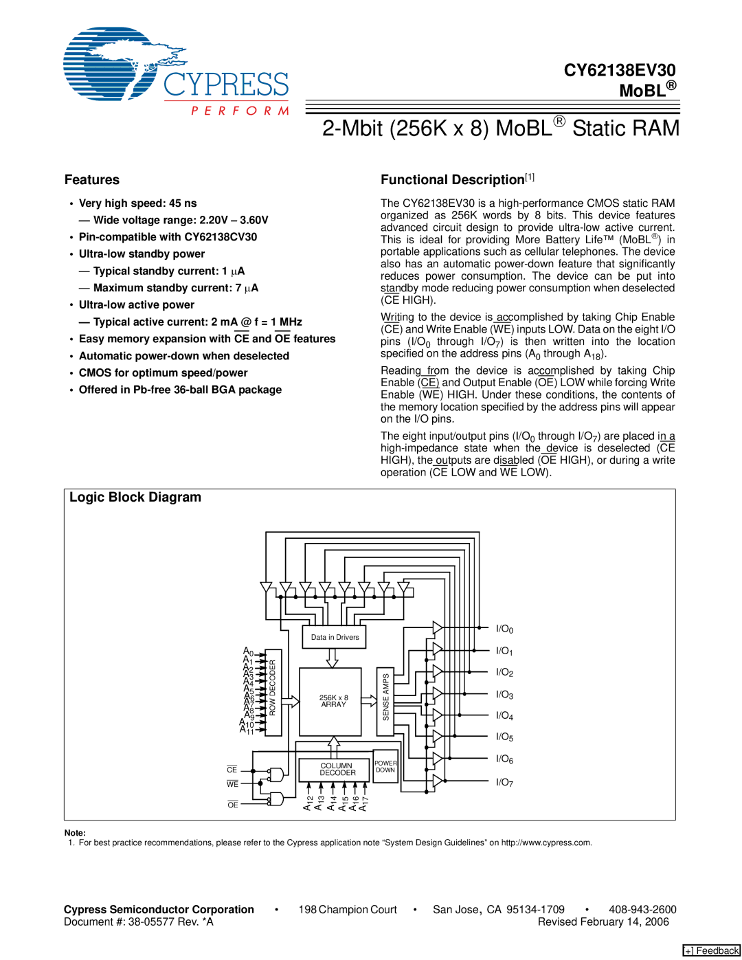
Writing to the device is accomplished by taking Chip Enable (CE) and Write Enable (WE) inputs LOW. Data on the eight I/O pins (I/O0 through I/O7) is then written into the location specified on the address pins (A0 through A18).
Reading from the device is accomplished by taking Chip Enable (CE) and Output Enable (OE) LOW while forcing Write Enable (WE) HIGH. Under these conditions, the contents of the memory location specified by the address pins will appear on the I/O pins.
The eight input/output pins (I/O0 through I/O7) are placed in a
Logic Block Diagram |
|
|
|
|
|
|
| Data in Drivers |
| I/O0 | |||
|
|
| ||||
A |
|
|
|
|
| I/O |
A10 | DECODER |
|
|
|
| 1 |
A |
|
|
|
| I/O2 | |
A23 |
|
|
| AMPS | ||
A |
|
|
|
| ||
A45 |
|
|
| I/O3 | ||
A |
| 256K x 8 |
| |||
A6 | ROW | SENSE |
| |||
A7 | ARRAY |
| ||||
A89 |
|
|
| I/O4 | ||
A10 |
|
|
|
|
|
|
A11 |
|
|
|
|
| I/O5 |
|
|
|
|
|
| |
CE |
| COLUMN | POWER | I/O6 | ||
| DOWN |
| ||||
| DECODER |
| ||||
|
|
| I/O7 | |||
WE |
|
|
|
|
| |
OE | 12 | 13 | 14 | 15 16 17 |
|
|
A A A A A A |
|
| ||||
|
|
| ||||
Note: |
|
|
|
|
|
|
1. For best practice recommendations, please refer to the Cypress application note “System Design Guidelines” on http://www.cypress.com.
Cypress Semiconductor Corporation | • | 198 Champion Court • San Jose, CA | • | |
Document #: |
| Revised February 14, 2006 | ||
[+] Feedback