MoBL® CY62148EV30

Switching Characteristics

(Over the Operating Range) [12]

Parameter


Description

- 45 (Ind’l/Auto-A)


- 55 [1]

Unit


Min

Max

Min


Max


Read Cycle


tRC


Read Cycle Time

45


55


ns

tAA


Address to Data Valid


45


55

ns

tOHA


Data Hold from Address Change

10


10


ns

tACE


LOW to Data Valid


45


55

ns

CE


tDOE


LOW to Data Valid


22


25

ns

OE


t


LOW to Low Z [13]

5


5


ns

OE


LZOE


t


HIGH to High Z [13, 14]


18


20

ns

OE


HZOE


t


LOW to Low Z [13]

10


10


ns

CE


LZCE


t


HIGH to High Z [13, 14]


18


20

ns

CE


HZCE


tPU


LOW to Power Up

0


0


ns

CE


tPD


HIGH to Power Up


45


55

ns

CE


Write Cycle [15]


tWC


Write Cycle Time

45


55


ns

tSCE


LOW to Write End

35


40


ns

CE


tAW


Address Setup to Write End

35


40


ns

tHA


Address Hold from Write End

0


0


ns

tSA


Address Setup to Write Start

0


0


ns

tPWE


Pulse Width

35


40


ns

WE


tSD


Data Setup to Write End

25


25


ns

tHD


Data Hold from Write End

0


0


ns

t


LOW to High Z [13, 14]


18


20

ns

WE


HZWE


t


HIGH to Low Z [13]

10


10


ns

WE


LZWE


Notes

12.Test Conditions for all parameters other than tri-state parameters assume signal transition time of 3 ns or less (1 V/ns), timing reference levels of VCC(typ)/2, input pulse levels of 0 to VCC(typ), and output loading of the specified IOL/IOH as shown in the “AC Test Loads and Waveforms” on page 4.

13.At any given temperature and voltage condition, tHZCE is less than tLZCE, tHZOE is less than tLZOE, and tHZWE is less than tLZWE for any given device.

14.tHZOE, tHZCE, and tHZWE transitions are measured when the output enter a high impedance state.

15.The internal write time of the memory is defined by the overlap of WE, CE = VIL. All signals must be ACTIVE to initiate a write and any of these signals can terminate a write by going INACTIVE. The data input setup and hold timing must be referenced to the edge of the signal that terminates the write.

Document #: 38-05576 Rev. *G

Page 5 of 12

[+] Feedback

Page 5
Image 5
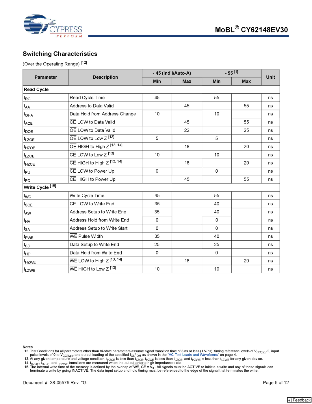
Cypress CY62148EV30 manual Switching Characteristics, Parameter Description Ind’l/Auto-A Unit Min, Read Cycle, Write Cycle

CY62148EV30 specifications

Cypress CY62148EV30 is a high-performance static random-access memory (SRAM) module renowned for its speed, low power consumption, and versatile applications in various electronic systems. With a storage capacity of 2 megabits (256K x 8 bits), this SRAM is ideal for developers seeking reliable memory solutions for high-speed computing tasks.

One of the standout features of the CY62148EV30 is its fast access time, which can be as low as 30 nanoseconds, allowing for rapid data retrieval and storage. This makes it particularly well-suited for applications that require quick response times, such as embedded systems, telecommunications, and automotive electronics.

The CY62148EV30 is built using advanced CMOS technology, resulting in a low standby current that significantly prolongs battery life in portable devices. This characteristic is crucial for mobile applications where power efficiency is paramount. The SRAM operates on a wide voltage range, typically between 2.7V and 3.6V, accommodating various system designs and enhancing compatibility with different voltage levels prevalent in modern electronics.

The device features a simple asynchronous interface with straightforward read and write operations. Its dual-port capability enables simultaneous access by multiple devices, enhancing performance in multi-processor or multi-user environments. This is particularly beneficial in networking applications where high-speed data exchange is essential.

Furthermore, the CY62148EV30 is designed with high reliability in mind. It includes built-in features such as data retention voltage, which ensures that data is preserved even in low power scenarios. Additionally, the device supports a wide temperature range, making it capable of functioning effectively in diverse environmental conditions.

The versatility of the CY62148EV30 extends to various applications, including cache memory for microcontrollers, buffers in communication systems, and data storage in digital signal processing environments. Its robust characteristics and performance capabilities make it a preferred choice for engineers seeking a high-quality, reliable SRAM solution.

In summary, the Cypress CY62148EV30 is an exemplary SRAM offering that combines high speed, low power consumption, and versatile application compatibility. With its advanced technology, fast access times, low standby current, and reliability features, it stands out as a key component in a myriad of modern electronic systems.