Contents
Main
8-Mbit (512K x 16) Static RAM
CY62157EV30 MoBL
Features
Functional Description
Logic Block Diagram
CY62157EV30 MoBL
Product Portfolio
Product Range
VCC Range (V) Speed (ns)
Pin Configuration
CY62157EV30 MoBL
The following picture shows the 48-ball VFBGA pinout.
Document #: 38-05445 Rev. *E Page 3 of 14
Pin Configuration (continued)
48-Ball VFBGA Top Vie w
Maximum Ratings
Operating Range
Electrical Characteristics
Capacitance
CY62157EV30 MoBL
Thermal Resistance
AC Test Loads and Waveforms
Data Retention Characteristics
Data Retention Waveform
CY62157EV30 MoBL
Switching Characteristics
CY62157EV30 MoBL
Switching Waveforms
Read Cycle No. 1 (Address Transition Controlled)[19, 20] Figure 3. Read Cycle No. 1
Read Cycle No. 2 (OE Controlled)[20, 21] Figure 4. Read Cycle No. 2
Document #: 38-05445 Rev. *E Page 8 of 14
Switching Waveforms
Write Cycle No. 3 (WE Controlled, OE LOW)[23] Figure 7. Write Cycle No. 3
Write Cycle No. 4 (BHE/BLE Controlled, OE LOW)[23] Figure 8. Write Cycle No. 4
Switching Waveforms
t
Truth Table
Ordering Information
Package Diagrams
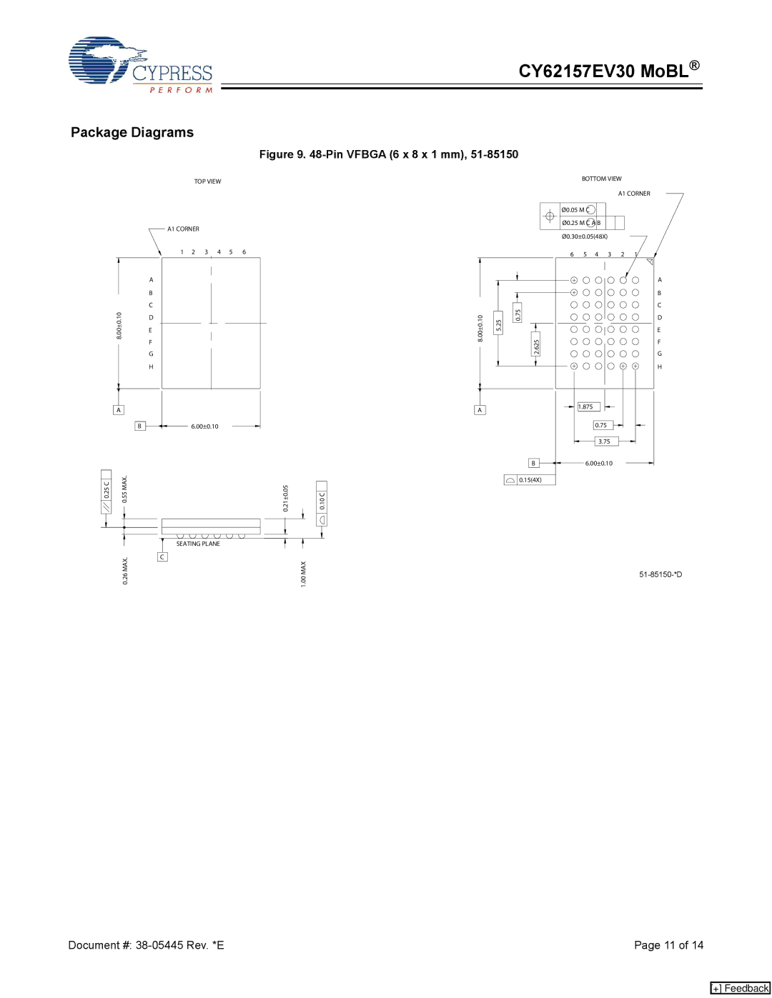
Figure 9. 48-Pin VFBGA (6 x 8 x 1 mm), 51-85150
51-85150-*D
Page
Figure 11. 48-Pin TSOP I (12 mm x 18.4 mm x 1.0 mm), 51-85183
Package Diagrams
51-85183-*A
Document History Page