Manuals
/
Cypress
/
Computer Equipment
/
Computer Hardware
Cypress
CY62157EV30
manual
Pin Tsop II
Models:
CY62157EV30
1
12
14
14
Download
14 pages
4.7 Kb
7
8
9
10
11
12
13
14
Electrical Characteristics
Logic Block Diagram
Pin Configuration
Inputs/Outputs Mode Power
Switching Waveforms
Page 12
Image 12
CY62157EV30 MoBL
®
Package Diagrams
(continued)
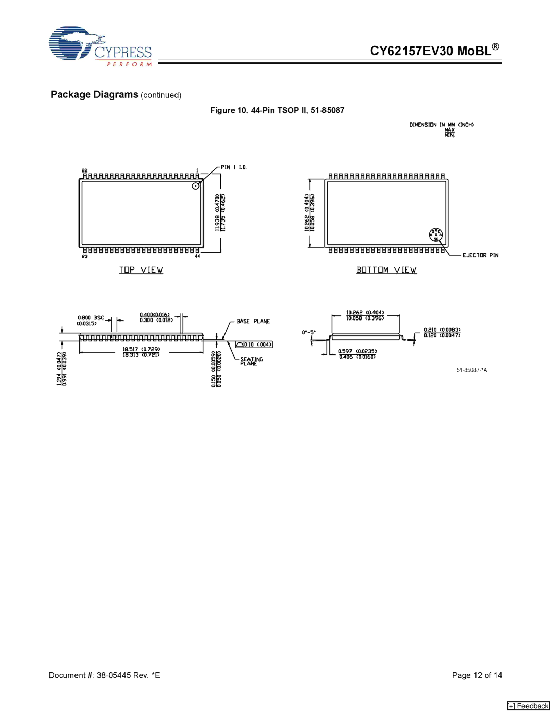
Figure 10.
44-Pin
TSOP II,
51-85087
51-85087-*A
Document #:
38-05445
Rev. *E
Page 12 of 14
[+] Feedback
Page 11
Page 13
Page 12
Image 12
Page 11
Page 13
Contents
Features
Logic Block Diagram
Functional Description1
Cypress Semiconductor Corporation
Pin Configuration
Product Portfolio
Following picture shows the 48-ball Vfbga pinout.3, 4
Ball Vfbga Top View
Electrical Characteristics
Maximum Ratings
Operating Range
Capacitance
Data Retention Characteristics
Thermal Resistance
AC Test Loads and Waveforms
Data Retention Waveform12
Switching Characteristics
Write Cycle
Switching Waveforms
Read Cycle No Address Transition Controlled19
Write Cycle No WE Controlled18, 22
Write Cycle No CE1 or CE2 Controlled18, 22
Write Cycle No WE Controlled, OE LOW23
Write Cycle No BHE/BLE Controlled, OE LOW23
Inputs/Outputs Mode Power
Truth Table
Ordering Information
BHE BLE
Package Diagrams
Pin Vfbga 6 x 8 x 1 mm
Pin Tsop II
Pin Tsop I 12 mm x 18.4 mm x 1.0 mm
Issue Date Orig. Change Description of Change
Document History
Document Number
REV ECN no
Top
Page
Image
Contents