CY62167EV30 MoBL®
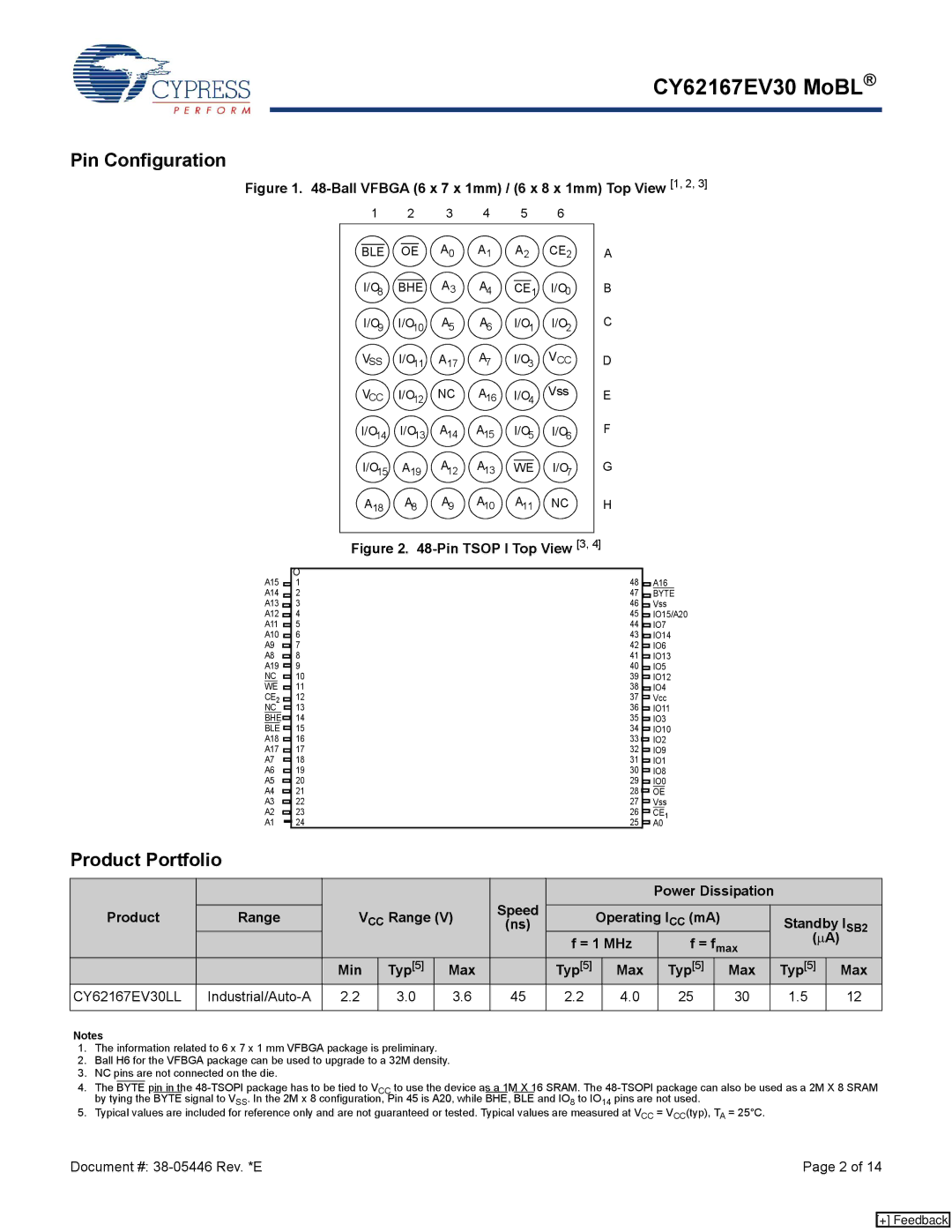
Pin Configuration
Figure 1. 48-Ball VFBGA (6 x 7 x 1mm) / (6 x 8 x 1mm) Top View [1, 2, 3]
1 | 2 | 3 | 4 | 5 |
| 6 |
| ||
BLE | OE | A0 | A1 | A2 |
| CE2 | A | ||
I/O | BHE | A3 | A | CE | 1 | I/O | B | ||
8 |
|
|
|
| 4 |
| 0 |
| |
I/O9 | I/O10 | A5 | A6 | I/O1 | I/O2 | C | |||
V | I/O | A | 17 | A | I/O |
| VCC | D | |
SS |
| 11 |
| 7 | 3 |
|
| ||
VCC | I/O | NC | A16 | I/O |
| Vss | E | ||
|
| 12 |
|
|
| 4 |
|
| |
I/O14 | I/O13 | A14 | A15 | I/O5 | I/O6 | F | |||
I/O | A | 19 | A | A13 | WE | I/O | G | ||
15 |
|
| 12 |
|
|
| 7 |
| |
A18 | A8 | A9 | A10 | A11 | NC | H | |||
Figure 2. |
| ||||||||
A15 |
|
|
|
|
| 1 | 48 |
|
|
| A16 | |||||||||||||
A14 |
|
|
|
|
| 2 | 47 |
|
|
| BYTE |
| ||||||||||||
A13 |
|
|
|
|
|
| 3 | 46 |
|
|
| Vss | ||||||||||||
|
|
|
|
|
| |||||||||||||||||||
A12 |
|
|
|
| 4 | 45 |
|
|
| IO15/A20 | ||||||||||||||
|
|
|
|
| ||||||||||||||||||||
A11 |
|
| 5 | 44 |
|
|
| IO7 | ||||||||||||||||
A10 |
|
|
| 6 | 43 |
|
|
| IO14 | |||||||||||||||
A9 |
|
|
|
|
|
|
| 7 | 42 |
|
|
| IO6 | |||||||||||
|
|
|
|
|
| |||||||||||||||||||
A8 |
|
| 8 | 41 |
|
|
| IO13 | ||||||||||||||||
A19 |
|
|
| 9 | 40 |
|
|
| IO5 | |||||||||||||||
NC |
|
|
| 10 | 39 |
|
|
| IO12 | |||||||||||||||
WE |
|
|
|
|
|
|
|
|
|
|
| 11 | 38 |
|
|
| IO4 | |||||||
CE2 |
|
|
|
|
|
|
|
|
|
|
| 12 | 37 |
|
|
| Vcc | |||||||
NC |
|
|
|
|
|
|
| 13 | 36 |
|
|
| IO11 | |||||||||||
BHE |
|
|
|
|
|
|
| 14 | 35 |
|
|
| IO3 | |||||||||||
BLE |
|
|
|
|
|
|
| 15 | 34 |
|
|
| IO10 | |||||||||||
A18 |
|
|
| 16 | 33 |
|
|
| IO2 | |||||||||||||||
A17 |
|
|
| 17 | 32 |
|
|
| IO9 | |||||||||||||||
A7 |
|
| 18 | 31 |
|
|
| IO1 | ||||||||||||||||
A6 |
|
| 19 | 30 |
|
|
| IO8 | ||||||||||||||||
|
|
|
|
| ||||||||||||||||||||
A5 |
|
| 20 | 29 |
|
|
| IO0 | ||||||||||||||||
A4 |
|
| 21 | 28 |
|
|
| OE | ||||||||||||||||
|
|
|
|
| ||||||||||||||||||||
A3 |
|
| 22 | 27 |
|
|
| Vss | ||||||||||||||||
|
|
|
|
| ||||||||||||||||||||
A2 |
|
| 23 | 26 |
|
|
| CE | 1 |
| ||||||||||||||
A1 |
|
|
|
| 24 | 25 |
|
|
| A0 |
| |||||||||||||
|
|
|
|
|
|
|
|
| ||||||||||||||||
Product Portfolio
|
|
|
|
|
|
|
|
| Power Dissipation |
|
|
| |||
Product | Range | VCC Range (V) | Speed |
| Operating ICC (mA) |
|
| Standby I | |||||||
(ns) |
|
|
| ||||||||||||
|
|
|
|
|
| f = 1 MHz | f = fmax |
| (μA) | SB2 | |||||
|
|
|
|
|
|
|
|
|
| ||||||
|
| Min | Typ[5] | Max |
| Typ[5] |
| Max | Typ[5] |
| Max |
| Typ[5] |
| Max |
CY62167EV30LL |
| 2.2 | 3.0 | 3.6 | 45 | 2.2 |
| 4.0 | 25 |
| 30 |
| 1.5 |
| 12 |
|
|
|
|
|
|
|
|
|
|
|
|
|
|
|
|
Notes
1.The information related to 6 x 7 x 1 mm VFBGA package is preliminary.
2.Ball H6 for the VFBGA package can be used to upgrade to a 32M density.
3.NC pins are not connected on the die.
4.The BYTE pin in the
5.Typical values are included for reference only and are not guaranteed or tested. Typical values are measured at VCC = VCC(typ), TA = 25°C.
Document #: | Page 2 of 14 |
[+] Feedback