CY62167EV30 MoBL®
Thermal Resistance
Tested initially and after any design or process changes that may affect these parameters.
Parameter | Description |
| Test Conditions | VFBGA | VFBGA | TSOP I | Unit |
| (6 x 7 x 1mm) | (6 x 8 x 1mm) | |||||
|
|
|
|
|
| ||
ΘJA | Thermal Resistance |
| Still Air, soldered on a 3 × 4.5 inch, | 27.74 | 55 | 60 | °C/W |
| (Junction to Ambient) |
|
|
|
|
| |
ΘJC | Thermal Resistance |
|
| 9.84 | 16 | 4.3 | °C/W |
| (Junction to Case) |
|
|
|
|
|
|
Shaded areas contain preliminary information. |
|
|
|
|
| ||
|
|
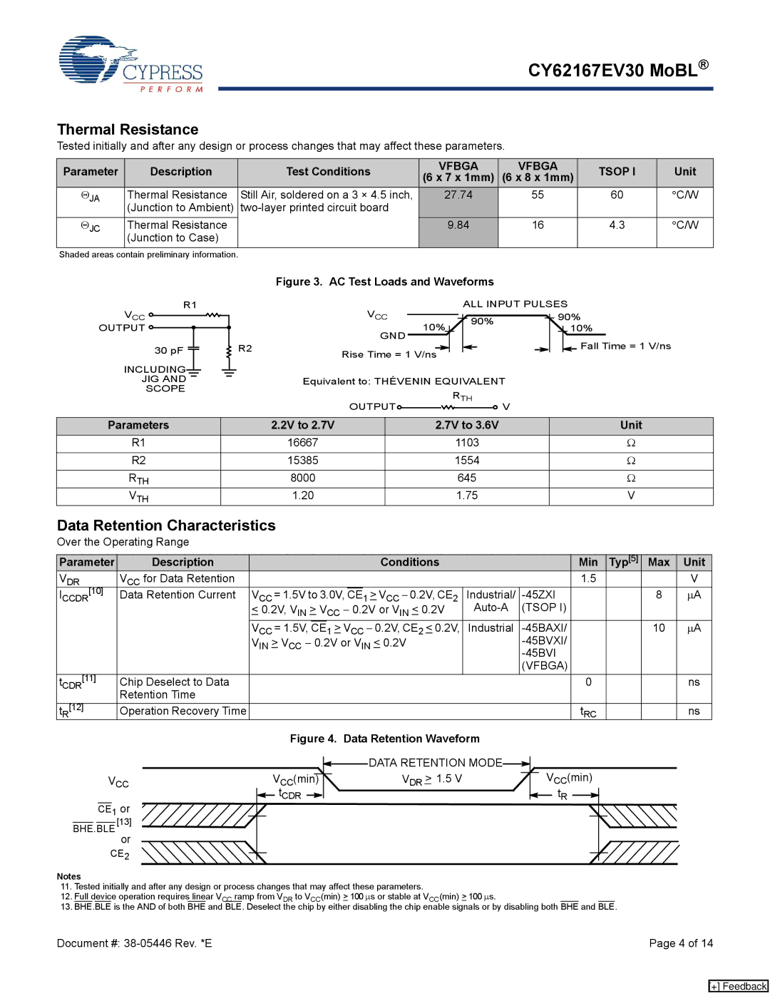
| Figure 3. AC Test Loads and Waveforms |
|
|
| |
R1
VCC ![]()
OUTPUT ![]()
30 pF ![]()
INCLUDING
JIG AND
SCOPE
| VCC |
|
|
|
|
|
|
|
|
|
| ALL INPUT PULSES | |||||||||
|
|
|
|
|
|
|
|
|
|
|
|
|
| 90% | |||||||
| 10% |
|
|
|
|
|
|
| 90% |
|
|
|
|
|
| 10% | |||||
|
|
|
|
|
|
|
|
|
|
|
|
|
|
|
| ||||||
R2 | GND |
|
|
|
|
|
|
|
|
|
|
|
|
|
|
|
|
| Fall Time = 1 V/ns | ||
|
|
|
|
|
|
|
|
|
|
|
|
|
|
|
|
| |||||
Rise Time = 1 V/ns |
|
|
|
|
|
|
|
|
|
|
|
|
|
| |||||||
|
|
|
|
|
|
|
|
|
|
|
|
|
|
|
| ||||||
| Equivalent to: THÉVENIN EQUIVALENT |
|
|
|
|
| |||||||||||||||
|
|
|
|
|
|
|
| RTH |
|
|
|
|
| ||||||||
| OUTPUT |
|
|
|
|
|
|
|
|
|
| V |
|
|
|
|
| ||||
|
|
|
|
|
|
|
|
|
|
|
|
|
|
| |||||||
Parameters | 2.2V to 2.7V | 2.7V to 3.6V | Unit |
R1 | 16667 | 1103 | Ω |
|
|
|
|
R2 | 15385 | 1554 | Ω |
|
|
|
|
RTH | 8000 | 645 | Ω |
VTH | 1.20 | 1.75 | V |
Data Retention Characteristics
Over the Operating Range
Parameter | Description |
|
|
|
| Conditions |
|
| Min | Typ[5] | Max | Unit |
VDR | VCC for Data Retention |
|
|
|
|
|
|
| 1.5 |
|
| V |
ICCDR[10] | Data Retention Current | VCC = 1.5V to 3.0V, | CE | 1 > VCC − 0.2V, CE2 | Industrial/ |
|
| 8 | μA | |||
|
| < 0.2V, VIN > VCC − 0.2V or VIN < 0.2V | (TSOP I) |
|
|
|
| |||||
|
| VCC = 1.5V, | CE | 1 > VCC − 0.2V, CE2 < 0.2V, | Industrial |
|
| 10 | μA | |||
|
| VIN > VCC − 0.2V or VIN < 0.2V |
|
|
|
|
| |||||
|
|
|
|
|
|
|
|
|
|
|
| |
|
|
|
|
|
|
|
| (VFBGA) |
|
|
|
|
tCDR[11] | Chip Deselect to Data |
|
|
|
|
|
|
| 0 |
|
| ns |
| Retention Time |
|
|
|
|
|
|
|
|
|
|
|
t [12] | Operation Recovery Time |
|
|
|
|
|
|
| t |
|
| ns |
R |
|
|
|
|
|
|
|
| RC |
|
|
|
VCC
CE1 or
BHE.BLE [13]
or
CE2
|
|
| Figure 4. Data Retention Waveform |
|
|
|
|
|
|
|
|
|
|
|
|
|
|
| ||||||||||
|
|
|
|
|
|
|
|
|
|
|
|
|
|
|
|
|
|
|
|
|
|
|
|
|
|
| ||
|
|
|
|
|
|
|
|
|
| DATA RETENTION MODE |
|
|
|
|
|
|
|
|
|
|
|
|
|
|
|
| ||
|
|
|
|
|
|
|
|
|
|
|
|
|
|
|
|
|
|
|
|
|
|
|
|
|
| |||
|
|
|
|
|
|
|
|
|
|
|
|
|
|
|
|
|
|
|
|
|
|
|
|
|
| |||
|
|
|
|
|
|
|
|
|
|
|
|
|
|
|
|
| VCC(min) |
|
|
|
| |||||||
|
| V (min) |
|
|
|
|
| V | DR | > 1.5 V |
|
|
|
|
|
|
|
|
| |||||||||
|
|
|
|
|
|
|
|
|
|
|
|
|
| |||||||||||||||
|
|
| CC |
|
|
|
|
|
|
|
|
|
|
|
|
|
|
|
|
|
|
|
|
| ||||
|
|
| tCDR |
|
|
|
|
|
|
|
|
|
|
|
|
|
|
| tR |
|
|
|
|
|
|
|
| |
|
|
|
|
|
|
|
|
|
| |||||||||||||||||||
|
|
|
|
|
|
|
|
|
|
|
|
|
|
|
|
|
|
|
|
|
|
|
| |||||
|
|
|
|
|
|
|
|
|
|
|
|
|
|
|
|
|
|
|
|
|
|
|
|
|
|
|
|
|
|
|
|
|
|
|
|
|
|
|
|
|
|
|
|
|
|
|
|
|
|
|
|
|
|
|
|
|
|
|
|
|
|
|
|
|
|
|
|
|
|
|
|
|
|
|
|
|
|
|
|
|
|
|
|
|
|
|
|
|
|
|
|
|
|
|
|
|
|
|
|
|
|
|
|
|
|
|
|
|
|
|
|
|
|
|
|
|
|
|
|
|
|
|
|
|
|
|
|
|
|
|
|
|
|
|
|
|
|
|
|
|
|
|
|
|
|
|
|
|
|
|
|
|
|
|
|
|
|
|
|
|
|
|
|
|
|
|
|
|
|
|
|
|
|
|
|
|
|
|
|
|
|
|
|
|
|
|
|
|
|
|
|
|
|
|
|
|
|
|
|
|
|
|
Notes
11.Tested initially and after any design or process changes that may affect these parameters.
12.Full device operation requires linear VCC ramp from VDR to VCC(min) > 100 μs or stable at VCC(min) > 100 μs.
13.BHE.BLE is the AND of both BHE and BLE. Deselect the chip by either disabling the chip enable signals or by disabling both BHE and BLE.
Document #: | Page 4 of 14 |
[+] Feedback