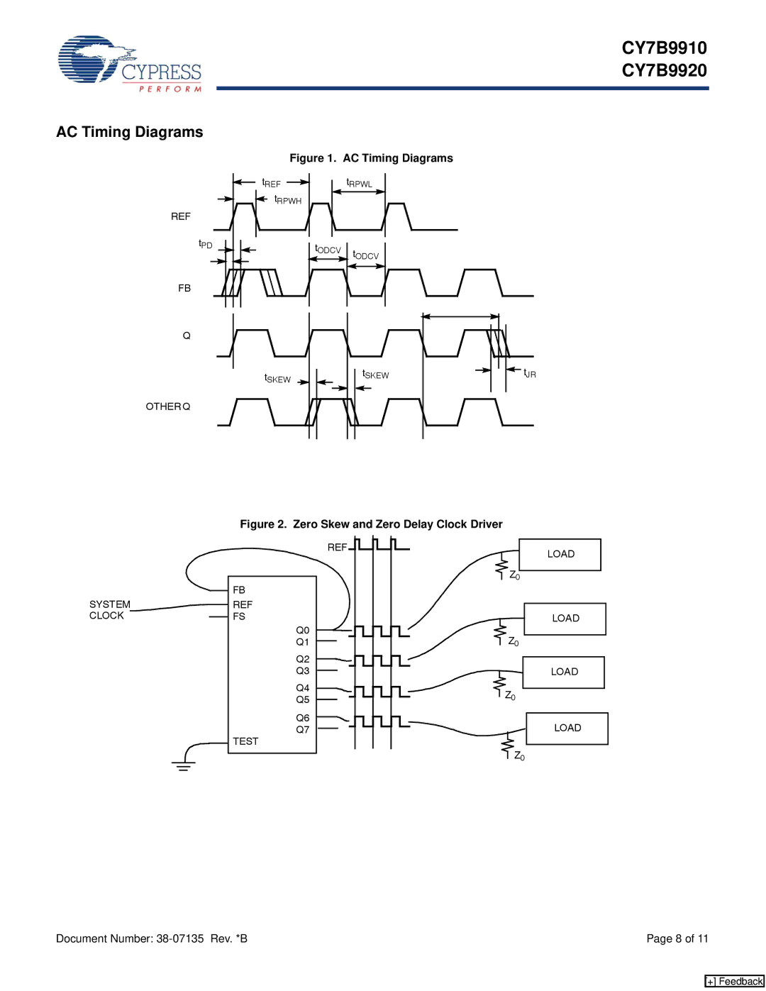
Manuals
/
Brands
/
Computer Equipment
/
Clock
/
Cypress
/
Computer Equipment
/
Clock
Cypress
CY7B9910, CY7B9920
AC Timing Diagrams
1
8
11
11
Download
11 pages, 387.39 Kb
CY7B9910
CY7B9920
Document Number: 38-07135 Rev. *B
Page 8 of 11
AC Timing Diagrams
Figure 1. AC Timing Diagrams
Figure 2. Zero Skew and Zero Delay Clock Driver
t
ODCV
t
ODCV
t
REF
REF
FB
Q
OTHER
Q
t
RPWH
t
RPWL
t
PD
t
SKEW
t
SKEW
t
JR
SYSTEM
CLOCK
FB
REF
FS
Q0
Q1
Q2
Q3
Q4
Q5
Q6
Q7
TEST
Z
0
LOAD
LOAD
LOAD
LOAD
REF
Z
0
Z
0
Z
0
[+] Feedback
[+] Feedback
Contents
Main
CY7B9910
Low Skew Clock Buffer
Features
Functional Description
Block Diagram Description
Phase Frequency Detector and Filter
CY7B9920
Pin Configuration
Test Mode
Pin Definitions
Maximum Ratings
Operating Range
Electrical Characteristics
AC Test Loads and Waveforms
Capacitance
Switching Characteristics
Page
CY7B9910 CY7B9920
Switching Characteristics
Document Number: 38-07135 Rev. *B Page 8 of 11
AC Timing Diagrams
[+] Feedback [+] Feedback
Figure 1. AC Timing Diagrams
Figure 2. Zero Skew and Zero Delay Clock Driver
CY7B9910 CY7B9920
Operational Mode Descriptions
CY7B9910
Ordering Information
Package Diagram
Document History