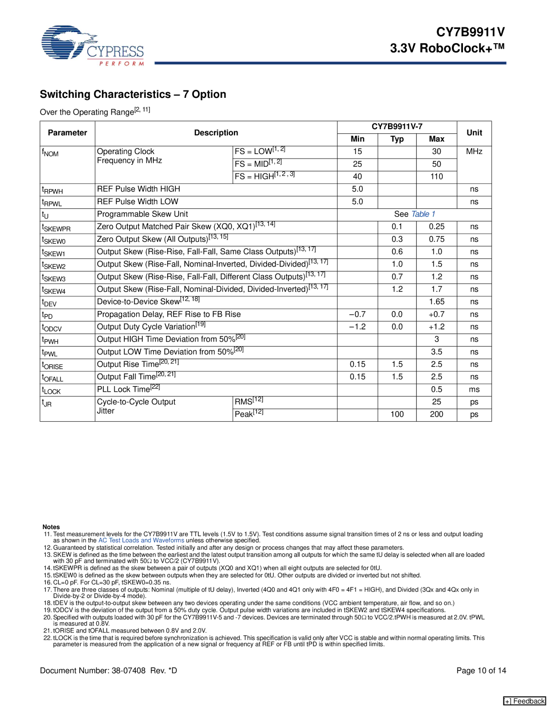
CY7B9911V 3.3V RoboClock+™
Switching Characteristics – 7 Option
Over the Operating Range[2, 11]
Parameter | Description |
|
|
| Unit | |||
Min |
| Typ |
| Max | ||||
|
|
|
|
|
| |||
|
|
|
|
|
|
|
|
|
fNOM | Operating Clock | FS = LOW[1, 2] | 15 |
|
|
| 30 | MHz |
| Frequency in MHz |
|
|
|
|
|
|
|
| FS = MID[1, 2] | 25 |
|
|
| 50 |
| |
|
| FS = HIGH[1, 2 , 3] | 40 |
|
|
| 110 |
|
tRPWH | REF Pulse Width HIGH |
| 5.0 |
|
|
|
| ns |
tRPWL | REF Pulse Width LOW |
| 5.0 |
|
|
|
| ns |
tU | Programmable Skew Unit |
|
|
| See Table 1 |
| ||
tSKEWPR | Zero Output Matched Pair Skew (XQ0, XQ1)[13, 14] |
|
| 0.1 |
| 0.25 | ns | |
tSKEW0 | Zero Output Skew (All Outputs)[13, 15] |
|
|
| 0.3 |
| 0.75 | ns |
t | Output Skew |
|
| 0.6 |
| 1.0 | ns | |
SKEW1 |
|
|
|
|
|
|
|
|
tSKEW2 | Output Skew |
|
| 1.0 |
| 1.5 | ns | |
t | Output Skew |
|
| 0.7 |
| 1.2 | ns | |
SKEW3 |
|
|
|
|
|
|
|
|
t | Output Skew |
|
| 1.2 |
| 1.7 | ns | |
SKEW4 |
|
|
|
|
|
|
|
|
tDEV |
|
|
|
|
| 1.65 | ns | |
tPD | Propagation Delay, REF Rise to FB Rise |
| 0.0 |
| +0.7 | ns | ||
t | Output Duty Cycle Variation[19] |
|
| 0.0 |
| +1.2 | ns | |
ODCV |
|
|
|
|
|
|
|
|
t | Output HIGH Time Deviation from 50%[20] |
|
|
|
| 3 | ns | |
PWH |
|
|
|
|
|
|
|
|
t | Output LOW Time Deviation from 50%[20] |
|
|
|
| 3.5 | ns | |
PWL |
|
|
|
|
|
|
|
|
t | Output Rise Time[20, 21] |
| 0.15 |
| 1.5 |
| 2.5 | ns |
ORISE |
|
|
|
|
|
|
|
|
tOFALL | Output Fall Time[20, 21] |
| 0.15 |
| 1.5 |
| 2.5 | ns |
tLOCK | PLL Lock Time[22] |
|
|
|
|
| 0.5 | ms |
t | RMS[12] |
|
|
|
| 25 | ps | |
JR | Jitter |
|
|
|
|
|
|
|
| Peak[12] |
|
| 100 |
| 200 | ps | |
Notes
11.Test measurement levels for the CY7B9911V are TTL levels (1.5V to 1.5V). Test conditions assume signal transition times of 2 ns or less and output loading as shown in the AC Test Loads and Waveforms unless otherwise specified.
12.Guaranteed by statistical correlation. Tested initially and after any design or process changes that may affect these parameters.
13.SKEW is defined as the time between the earliest and the latest output transition among all outputs for which the same tU delay is selected when all are loaded with 30 pF and terminated with 50Ω to VCC/2 (CY7B9911V).
14.tSKEWPR is defined as the skew between a pair of outputs (XQ0 and XQ1) when all eight outputs are selected for 0tU.
15.tSKEW0 is defined as the skew between outputs when they are selected for 0tU. Other outputs are divided or inverted but not shifted.
16.CL=0 pF. For CL=30 pF, tSKEW0=0.35 ns.
17.There are three classes of outputs: Nominal (multiple of tU delay), Inverted (4Q0 and 4Q1 only with 4F0 = 4F1 = HIGH), and Divided (3Qx and 4Qx only in
18.tDEV is the
19.tODCV is the deviation of the output from a 50% duty cycle. Output pulse width variations are included in tSKEW2 and tSKEW4 specifications.
20.Specified with outputs loaded with 30 pF for the
21.tORISE and tOFALL measured between 0.8V and 2.0V.
22.tLOCK is the time that is required before synchronization is achieved. This specification is valid only after VCC is stable and within normal operating limits. This parameter is measured from the application of a new signal or frequency at REF or FB until tPD is within specified limits.
Document Number: | Page 10 of 14 |
[+] Feedback